Semiconductor light-emitting element and method of manufacturing the same

A light-emitting element and manufacturing method technology, applied in the direction of semiconductor lasers, electrical components, laser components, etc., can solve the problem of high contact resistance, increase in operating voltage of semiconductor light-emitting elements, reduction of contact area between p-type contact layer and p-side electrode, etc. problem, to achieve the effect of increasing the contact area and lowering the operating voltage

Inactive Publication Date: 2010-11-03
MITSUBISHI ELECTRIC CORP
View PDF1 Cites 6 Cited by
  • Summary
  • Abstract
  • Description
  • Claims
  • Application Information

AI Technical Summary

Problems solved by technology

[0004] In the manufacturing method of above-mentioned existing semiconductor light-emitting element, owing to cover the part of the upper surface of the p-type contact layer that is formed on the ridge top by insulating film, so, there is the contact area of ​​p-type contact layer and p-side electrode to reduce, And the problem that the operating voltage of the semiconductor light-emitting element increases
In particular, in blue-violet semiconductor light-emitting elements, since the contact resistance of nitride semiconductors such as GaN used in the p-type contact layer is higher than that of III-V compound semiconductors such as GaAs used in the p-type contact layer of red semiconductor light-emitting elements Due to the high contact resistance of the p-type contact layer and the p-side electrode, there is a problem that the operating voltage of the semiconductor light-emitting element is significantly increased.

Method used


Image

  • Semiconductor light-emitting element and method of manufacturing the same
  • Semiconductor light-emitting element and method of manufacturing the same
  • Semiconductor light-emitting element and method of manufacturing the same

Examples


Embodiment approach 1

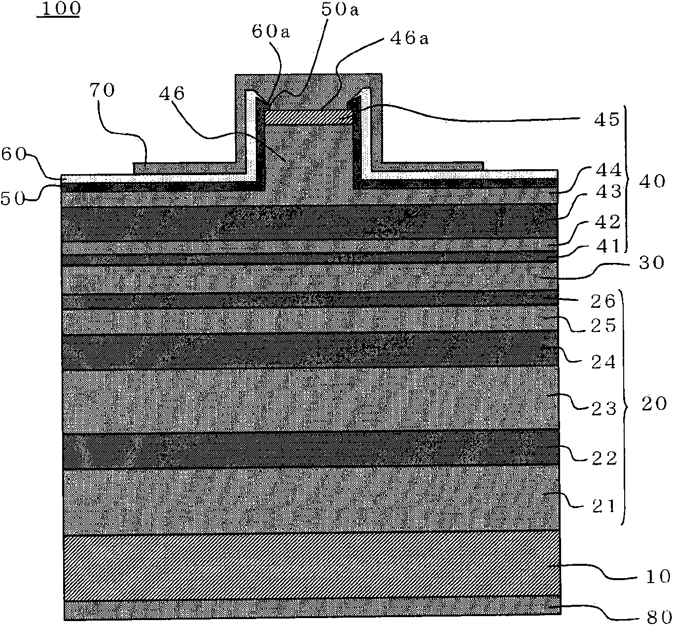
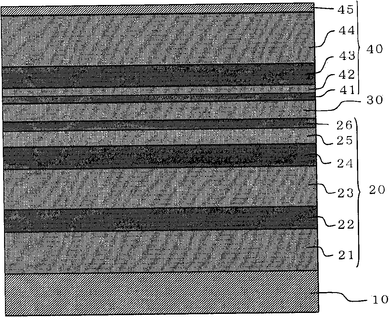
[0033] figure 1 It is a cross-sectional view illustrating the structure of the semiconductor light emitting element in Embodiment 1 of the present invention, Figure 2 ~ Figure 6 It is a cross-sectional view illustrating a method of manufacturing a semiconductor light emitting element in Embodiment 1 of the present invention.

[0034] First, refer to figure 1 The structure of the semiconductor light emitting element in Embodiment 1 will be described.

[0035] figure 1 In the semiconductor laser element 100 as a semiconductor light emitting element, on an n-type GaN substrate 10, as an n-type (first conductivity type) semiconductor layer 20, an n-type GaN buffer layer 21 with a layer thickness of 1000 nm, a layer thickness 400nm n-type Al 0.07 Ga 0.93 N-clad 22, n-type Al with a layer thickness of 1000nm 0.045 Ga 0.955 N-clad layer 23, n-type Al with a layer thickness of 300nm 0.015 Ga 0.985 N-clad layer 24, n-type GaN light guide layer 25 with a layer thickness of ...

Embodiment approach 2

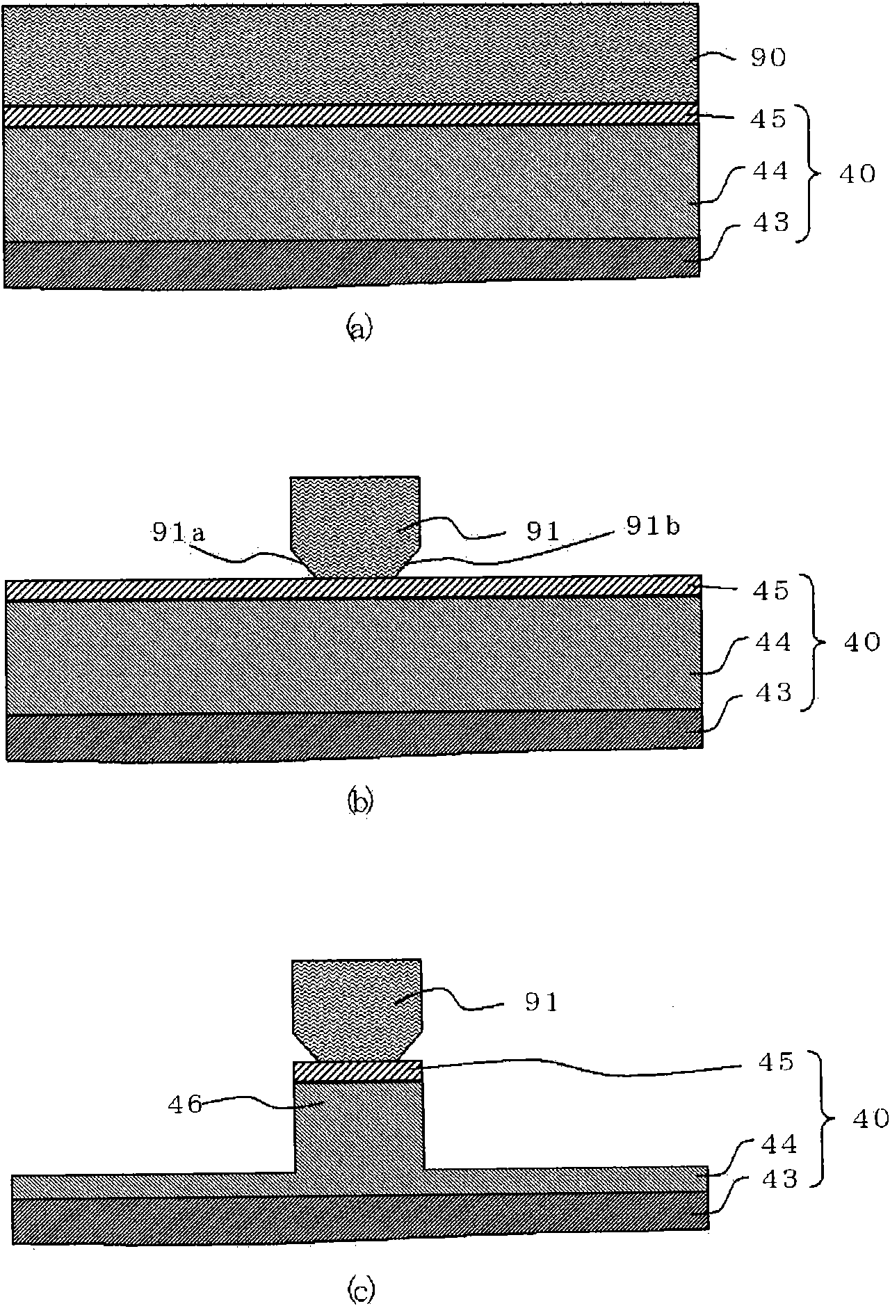
[0081] Figure 7 It is a cross-sectional view showing the structure of the semiconductor light emitting element in Embodiment 2 of the present invention. In the semiconductor light-emitting element in Embodiment 1, the metal film 60 is formed of a single-layer metal film, but in the semiconductor light-emitting element in Embodiment 2, the metal film 60 is formed of multiple metal films.

[0082] Figure 7 In the second embodiment, the metal film 60 provided on the semiconductor laser device 200 which is a semiconductor light-emitting device in the second embodiment is formed by the first metal film 61 provided in contact with the p-side electrode 70 made of Pd and the first metal film 61 made of SiO. 2 The second metal film 62 formed in contact with the insulating film 50 is formed in two layers. Here, the first metal film 61 is formed of Au, and the second metal film 62 is formed of Cr or Ti. Except for these points, the semiconductor laser element 200 in the second embod...

Embodiment approach 3

[0089] Figure 8 It is a cross-sectional view showing the structure of the semiconductor light emitting element in Embodiment 3 of the present invention.

[0090] Figure 8 In the semiconductor laser element 300 which is a semiconductor light-emitting element in the third embodiment, the opening width of the first opening 50 a provided in the insulating film 50 is set to be wider than the opening width of the second opening 60 a provided in the metal film 60 . Wide. Except for this point, the semiconductor laser element 300 has the same structure as the semiconductor laser element 100 of the first embodiment.

[0091] In addition, in the semiconductor structural element 300 , the steps other than the insulating film etching step described later are the same steps as those shown in Embodiment 1, and therefore description thereof will be omitted.

[0092] In the insulating film etching process, using the metal film 60 as a mask, dry etching or wet etching is performed by SiO ...


PUM


Abstract

The invention provides a semiconductor light-emitting element and a manufacturing method capable of easily enlarging the contact area of a p side electrode and a p type contact layer, furthermore the semiconductor light-emitting element with low operation voltage is obtained. An overhanging-shaped resist pattern (91) on a ridge waveguide top face (46a) is used and a metal film (60) is deposited on the ridge waveguide top face in the way of forming a step with an end part of an insulation film (50). The metal film is used as the mask to etch the insulation film (50) of the ridge waveguide top face (46a). Thus the opening width of an opening part (50a) of the insulation film (50) is enlarged without setting a new mask step and the contact area of the p side electrode (70) and the p type contact layer (45) is enlarged.

Description

technical field [0001] The present invention relates to a manufacturing method of a semiconductor light-emitting element and a semiconductor light-emitting element, in particular to a ridge-type semiconductor laser element and a manufacturing method thereof. Background technique [0002] A conventional method for manufacturing a ridge-type semiconductor laser device includes forming an overhang-shaped resist with a part of the upper surface exposed on the upper surface of a p-type GaN contact layer formed on the top of a ridge of an AlGaInN-based compound semiconductor. The step of forming an insulating film so as to cover the exposed portion on the resist and the upper surface of the p-type contact layer; removing the resist to peel off the insulating film formed on the resist The process of forming a p-side electrode on the opening of the p-type contact layer and the insulating film, thereby improving the yield in the above-mentioned lift-off process (for example, refer to...

Claims


Application Information

Patent Timeline
Patent Type & Authority Applications(China)
IPC IPC(8): H01S5/00
CPCH01S5/0425H01S5/2214H01S5/2009H01S5/2201H01S5/34306H01S5/3213H01S5/04254H01S5/04252
Inventor 冈贵郁阿部真司川崎和重堀江淳一佐久间仁
Owner MITSUBISHI ELECTRIC CORP
Why Eureka
Try Eureka