
Nitride-oxide-silicon bipolar resistive random access memory based on non-stoichiometry ratio and preparation method thereof

A resistive memory, resistive switching technology, applied in electrical components and other directions, can solve problems such as increasing process steps

Active Publication Date: 2010-11-24
SEMICONDUCTOR MANUFACTURING INTERNATIONAL (BEIJING) CORP +1
View PDF2 Cites 7 Cited by
  • Summary
  • Abstract
  • Description
  • Claims
  • Application Information

AI Technical Summary

Problems solved by technology

Such substances are generally compatible with the CMOS process and can exhibit good resistive switching characteristics. However, compared with conventional processes, some process steps are often required

Method used


Image

  • Nitride-oxide-silicon bipolar resistive random access memory based on non-stoichiometry ratio and preparation method thereof
  • Nitride-oxide-silicon bipolar resistive random access memory based on non-stoichiometry ratio and preparation method thereof
  • Nitride-oxide-silicon bipolar resistive random access memory based on non-stoichiometry ratio and preparation method thereof

Examples


Embodiment Construction

[0020] The present invention will be further described below through specific embodiments in conjunction with the accompanying drawings.

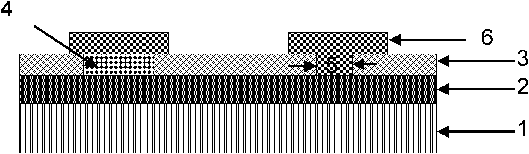
[0021] The schematic diagram of the cross-sectional structure of the resistive memory of the present invention is as follows: figure 1 As shown, the preparation process of the resistive variable memory of this example is described below in combination with the schematic cross-sectional structure.

[0022] 1) First, a layer of W metal is prepared on the silicon substrate 1 by physical vapor deposition (PVD) method or other film-forming methods in the IC process, and the substrate is formed by etching, etching or stripping using standard photolithography techniques. The electrode is patterned to form the bottom electrode 2 .

[0023] 2) Prepare the isolation layer by PECVD or ALD or PVD or MOCVD;

[0024] 3) Preparation of resistive material layer SiO by PECVD x N y , where x=0.4, y=1.

[0025] 3) The bottom electrode lead-out hole is de...


PUM

PropertyMeasurementUnit
thicknessaaaaaaaaaa

Abstract

The invention provides a bipolar resistive random access memory of a nitride-oxide-silicon (SiOxNy) resistive random material containing rich silicon based on non-stoichiometry ratio and a preparation method thereof, belonging to the technical field of super-large-scale integration. The resistive random access memory comprises a top electrode, a resistive random material layer, a bottom electrode and a substrate, wherein the resistive random material layer is the nitrogen oxide of silicon (SiOxNy), and x and y in the SiOxNy meet the conditions of (2x+3y)<4, x>=0, and y>=0; the bottom electrode is metal or a conducting material such as Cu, W, Pt and the like; and the top electrode is metal or a conducting material such as Ti, TiN, Al, AlCu and the like generating chemical reaction with the nitrogen oxide of silicon. In the invention, by controlling the components of the nitrogen oxide of silicon, the silicon content is relatively larger, and more defects, vacancies, such as nitrogen vacancy, oxygen vacancy and the like are introduced, thereby obtaining a stable bipolar device.

Description

technical field [0001] The invention belongs to the technical field of ultra-large-scale integrated circuits, and in particular relates to a non-volatile resistive memory, which realizes the purpose of storing data 0 and 1 by changing the resistance value. Background technique [0002] With the continuous advancement of integrated circuit technology nodes, the FLASH technology based on the traditional floating gate structure will face technical challenges that cannot be scaled down. Resistive RAM (RRAM) based on MIM (Metal-Insulator-Metal) structure has the potential to replace traditional memory due to its simple structure, easy fabrication, small size, high integration, fast erasing and writing speed, and low power consumption. Therefore, it has attracted much attention from academia and industry. Different from FLASH of the traditional floating gate structure, which relies on the amount of charge to store information 0 and 1, RRAM uses its high resistance and low resista...

Claims


Application Information

Patent Timeline
Patent Type & Authority Applications(China)
IPC IPC(8): H01L45/00
Inventor 张丽杰黄如潘越
Owner SEMICONDUCTOR MANUFACTURING INTERNATIONAL (BEIJING) CORP
Learn More