Making method and system of semi-conductor device

A manufacturing method and semiconductor technology, which are applied in the manufacture of semiconductor/solid-state devices, electrical components, circuits, etc., can solve the problems of limited increase, limit the improvement of HTO quality, limited number of structures, etc., and achieve the effect of improving quality and performance.

Inactive Publication Date: 2010-12-08
SEMICON MFG INT (SHANGHAI) CORP
View PDF2 Cites 2 Cited by
  • Summary
  • Abstract
  • Description
  • Claims
  • Application Information

AI Technical Summary

Problems solved by technology

However, due to the existence of problems such as insufficient reaction, there may be defects in the structure of the HTO produced by the above-mentioned traditional scheme, for example, for the silicon dioxide (SiO2) of the defect structure in HTO 2 ), one silicon atom may only be combined with one oxygen atom, so after HTO is obtained, it is generally necessary to process HTO to improve the structure of HTO and improve the quality of HTO
[0008] The inventors of the present application analyzed and concluded that: for the scheme provided by the patent-related document US6830974, since oxygen is difficult to decompose into oxygen atoms at about 900°C, the number of defect structures of HTO corrected by this scheme is limited, which limits the improvement of HTO quality
For the scheme provided by the patent-related document US20060211270, some of the decomposed oxygen atoms will be combined with N 2 O reacts to generate nitric oxide (NO). Therefore, although the number of oxygen atoms provided by this scheme has increased and the number of corrected defect structures has increased, the increase is still very limited, which still limits the improvement of HTO quality.
[0009] Since the quality of HTO seriously affects the performance of its semiconductor devices, the existing solutions limit the improvement of HTO quality, which also limits the improvement of semiconductor device performance.

Method used


Image

  • Making method and system of semi-conductor device
  • Making method and system of semi-conductor device
  • Making method and system of semi-conductor device

Examples


Embodiment Construction

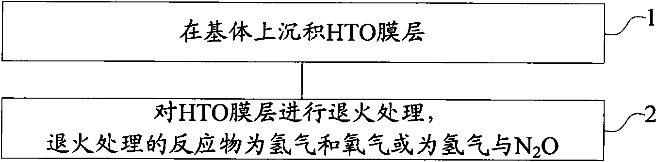
[0017] In view of the problems mentioned in the background technology, the embodiment of the present invention proposes the following design ideas: if after the HTO is formed, an appropriate reactant is selected for annealing treatment to provide more oxygen atoms to enter the HTO to correct the defect structure in the HTO, Then, compared with the prior art, the number of corrected defect structures can be greatly increased, thereby improving the quality of the HTO, and further improving the quality of the semiconductor device.

[0018] figure 1 The flowchart of the semiconductor device manufacturing method provided by the embodiment of the present invention, combined with this figure, based on the above design idea, the manufacturing method includes steps:

[0019] Step 1, depositing the HTO film layer on the substrate. The substrate represents the structure that has been produced before depositing the HTO film layer in the process of manufacturing semiconductor devices. The ...


PUM


Abstract

The invention provides making method and system of a semi-conductor device. The semi-conductor device comprises an HTO (High Temperature Oxidation) to improve the quality of the HTO and further the performance of the semi-conductor device. The method comprises the following steps of depositing an HTO film layer on a matrix; and treating the HTO film layer by annealing treatment, wherein reactants in the annealing treatment are hydrogen and oxygen or the hydrogen and nitrogen oxide.

Description

technical field [0001] The invention relates to the field of semiconductor manufacturing, in particular to a semiconductor device manufacturing method and system. Background technique [0002] High temperature oxide film (HTO, High Temperature Oxide) is widely used in various semiconductor integrated circuits such as logic products, dynamic random access memory (DRAM, Dynamic Random Access Memory) and flash memory (Flash). [0003] The traditional scheme usually adopts low-temperature chemical vapor deposition (LPCVD, Low Pressure Chemical Vapor Deposion) method to make HTO, and in this scheme, HTO is generally made of dichlorosilane (SiH 2 Cl 2 ) or silane (SiH4) and nitrogen oxide (N 2 O) react at a temperature of 700 to 800 degrees Celsius (°C) to obtain silicon dioxide (SiO 2 ) or silicon tetroxide (SiO 4 )Wait. However, due to the existence of problems such as insufficient reaction, there may be defects in the structure of the HTO produced by the above-mentioned tr...

Claims


Application Information

Patent Timeline
IPC IPC(8): H01L21/316H01L21/3105H01L21/8247H01L21/00
Inventor 宋化龙史运泽李亮沈忆华
Owner SEMICON MFG INT (SHANGHAI) CORP
Why Eureka
Try Eureka