
Active matrix/organic light emitting display and manufacturing method thereof

A light-emitting display and active matrix technology, applied in the field of active-matrix organic light-emitting display and its manufacturing, can solve the problems that cannot fully meet the application requirements of AMOLED, it is difficult to drive TFT, etc., and achieve overall performance and high carrier migration. rate, good consistency

Inactive Publication Date: 2010-12-22
KUNSHAN NEW FLAT PANEL DISPLAY TECH CENT +2
View PDF1 Cites 11 Cited by
  • Summary
  • Abstract
  • Description
  • Claims
  • Application Information

AI Technical Summary

Problems solved by technology

Therefore, it is difficult to obtain a switching TFT with high carrier mobility and a driving TFT with good consistency by using ELA or SPC technology alone, which cannot fully meet the application requirements of AMOLED.

Method used


Image

  • Active matrix/organic light emitting display and manufacturing method thereof
  • Active matrix/organic light emitting display and manufacturing method thereof
  • Active matrix/organic light emitting display and manufacturing method thereof

Examples


Embodiment

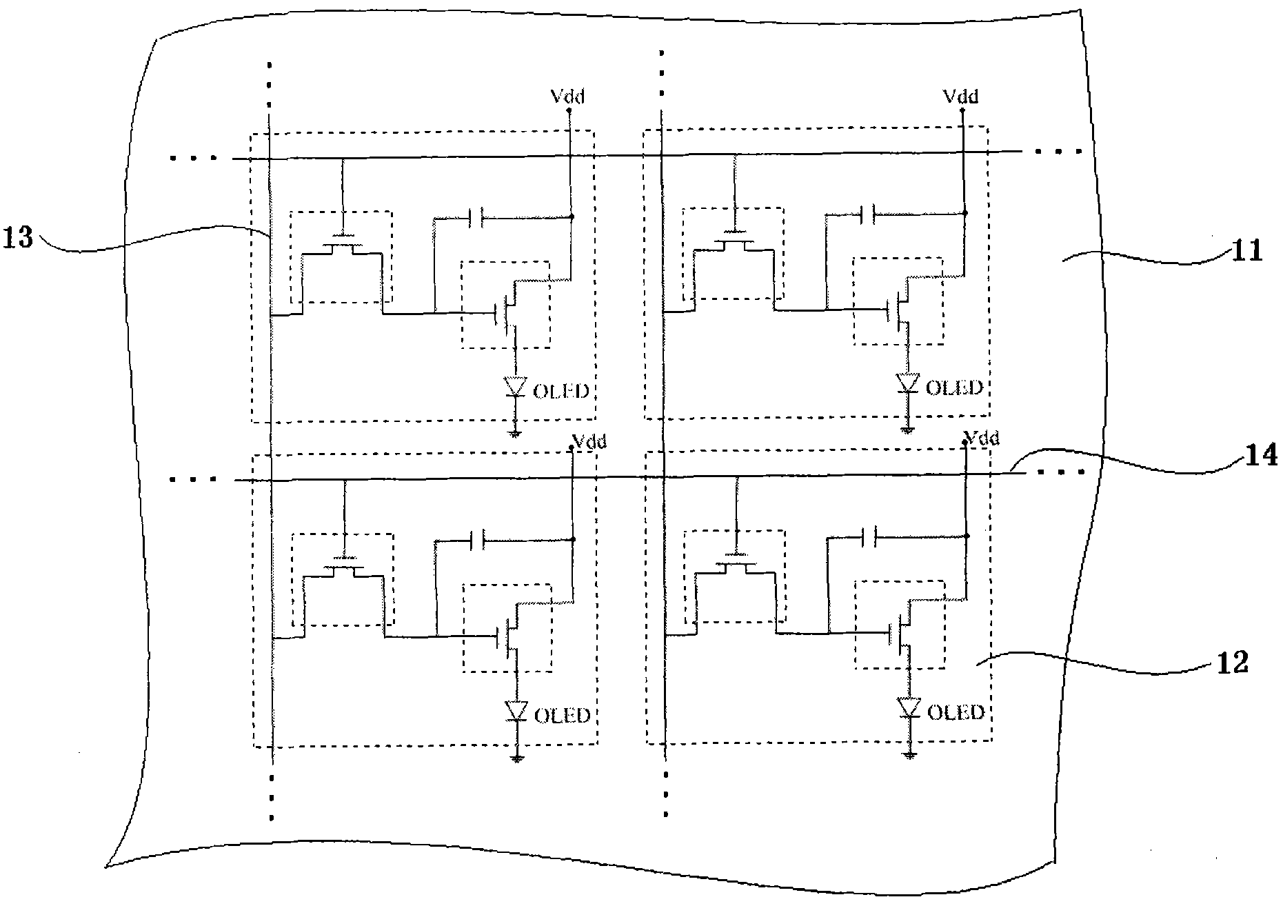
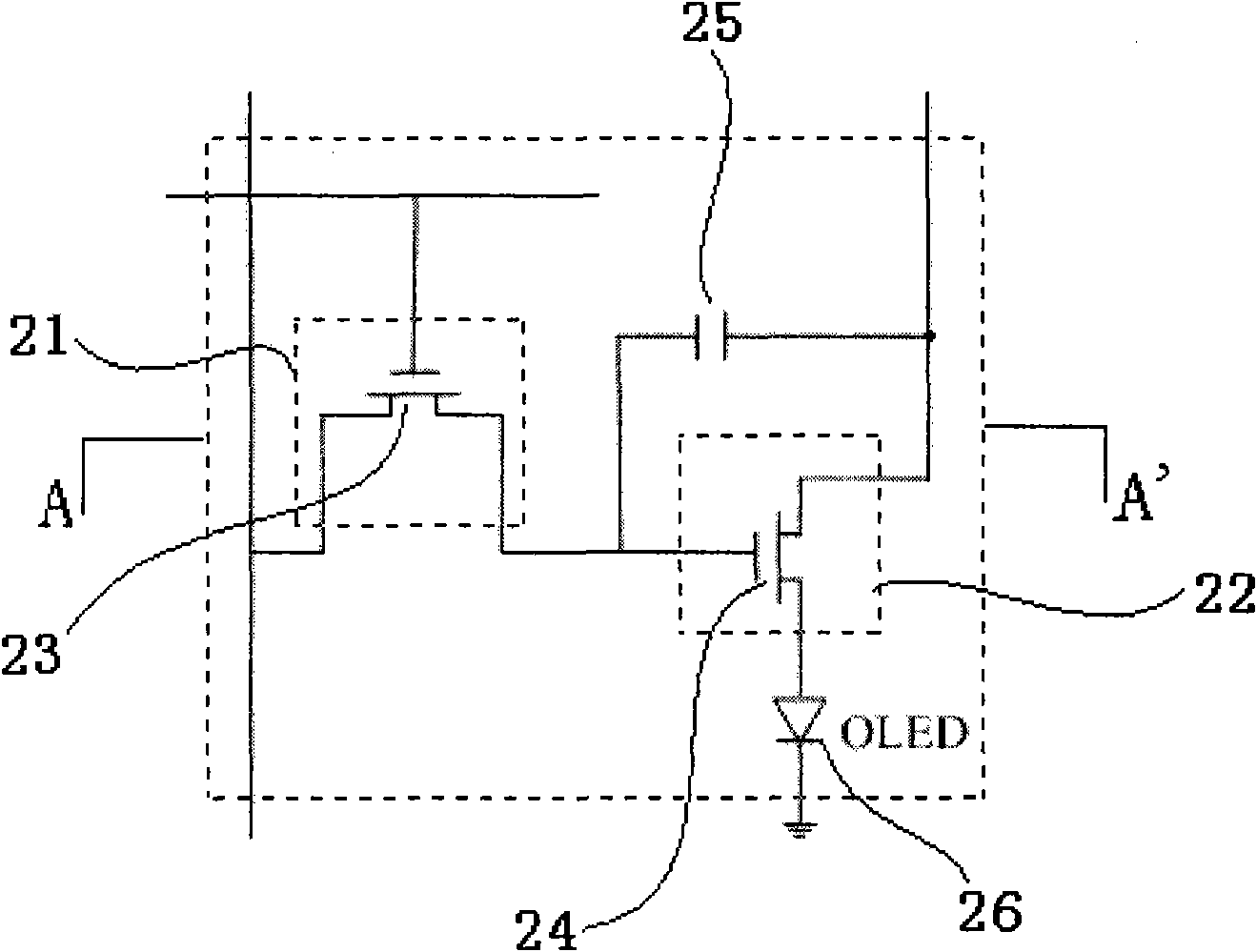
[0030] figure 1 It is a schematic diagram of a local circuit structure of an array substrate of an active matrix organic light-emitting display. As shown in the figure, the array substrate includes a glass substrate 11, and a plurality of pixels 12 arranged on the substrate are arranged in a matrix and arranged in parallel between the pixels A plurality of data lines 13 and a plurality of scan lines 14 arranged between the pixels and perpendicular to the data lines are arranged in parallel. figure 2 for figure 1 The schematic diagram of the enlarged structure of the pixel 12, as shown in the figure, the pixel 12 has a switching area 21 and a driving area 22 in the pixel area, the switching area 21 has a switching thin film transistor 23, and the driving area 22 It has a driving thin film transistor 24 , and also includes a storage capacitor 25 and an organic light emitting device 26 . The carrier mobility of the driving thin film transistor 24 is about 25 cm 2 / Vs, the car...


PUM


Abstract

The invention relates to an active matrix / organic light emitting display and a manufacturing method thereof, in particular to a low-temperature polysilicon display panel and a manufacturing method thereof. In the technical scheme of the invention, a switch thin-film transistor (TFT) with high carrier mobility is obtained in a switch area in a pixel and a drive TFT with good consistency is obtained in a drive area by way of double crystallization, namely solid-phase crystallization and local laser crystallization, thus realizing improvement of the overall property of the active matrix / organic light emitting display.

Description

technical field [0001] The invention relates to an active matrix organic light-emitting display and a manufacturing method thereof, in particular to a low-temperature polysilicon display panel and a manufacturing method thereof. Background technique [0002] Low temperature polysilicon thin film transistors (LTPS TFTs) have been commonly used in flat panel displays, such as active matrix liquid crystal displays (AMLCDs), active matrix organic light emitting displays (AMOLEDs), and the like. This type of display generally deposits an amorphous silicon layer (a-Si) on a glass substrate first, and then crystallizes the amorphous silicon through heat treatment to form a polysilicon film (p-Si) with smoother and larger grains. A thin film transistor (TFT) array is fabricated using a polysilicon film. Currently, solid phase crystallization (SPC) and excimer laser annealing (ELA) are mainstream technologies for LTPS crystallization technologies. Among them, the TFT obtained by us...

Claims


Application Information

Patent Timeline
Patent Type & Authority Applications(China)
IPC IPC(8): H01L21/82H01L27/32H01L51/52H01L51/56
Inventor 黄秀颀邱勇高孝裕魏朝刚
Owner KUNSHAN NEW FLAT PANEL DISPLAY TECH CENT
Learn More