Flash memory manufacturing method

A manufacturing method and memory technology, applied in semiconductor/solid-state device manufacturing, electrical components, circuits, etc., can solve the problems of difficult programming operation of chips, low current, low mobility, etc., and achieve good isolation effect

Inactive Publication Date: 2010-12-22
SEMICON MFG INT (SHANGHAI) CORP
View PDF0 Cites 1 Cited by
  • Summary
  • Abstract
  • Description
  • Claims
  • Application Information

AI Technical Summary

Problems solved by technology

However, the flash memory works by controlling the electrons, so the cells close to the STI have low mobility, and the working current will be lower than that far away from the STI, and the programming ability is also low.
Under the same operating conditions, the memory cells near the STI cannot work as well as the memory cells far away from the STI, which makes it difficult to program the chip and reduces the performance of the chip

Method used


Image

  • Flash memory manufacturing method
  • Flash memory manufacturing method
  • Flash memory manufacturing method

Examples


Embodiment Construction

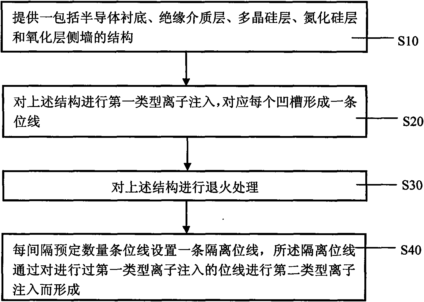
[0035] In order to better understand the technical content of the present invention, specific embodiments are given and described as follows in conjunction with the accompanying drawings.
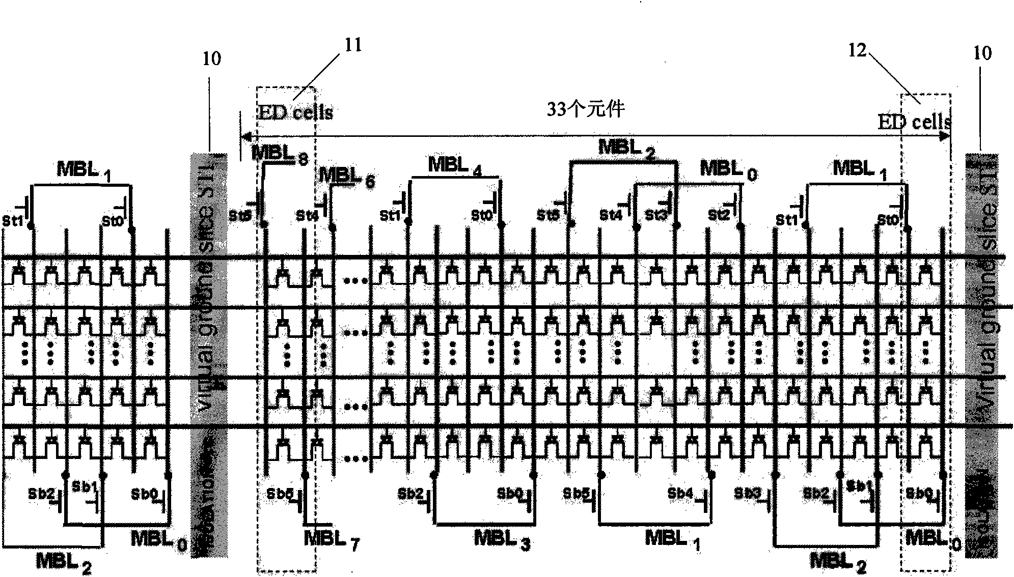
[0036] The core idea of ​​the present invention is that, based on the existing storage structure of the flash memory, through different types of ion implantation, a bit with an isolation effect is formed between groups composed of a predetermined number (16-50) of storage cells. line, thereby replacing the shallow trench isolation structure used in the prior art, while achieving the same effect of using shallow trench isolation to solve adjacent interference, it can also avoid the generation of mechanical stress, thereby improving the performance of the flash memory .

[0037] The invention proposes a manufacturing method of flash memory, which can achieve the same effect of using shallow trench isolation without generating mechanical stress.

[0038] Please refer to image 3 , image 3 ...


PUM


Abstract

The invention provides a flash memory manufacturing method which comprises the following steps: providing a structure comprising a semiconductor substrate, an insulating medium layer, a polycrystalline silicon layer, a silicon nitride layer and an oxide layer side wall; carrying out first type ion implantation on the structure, and forming a plurality of bit lines corresponding to each groove; carrying out annealing treatment on the structure; and arranging isolated bit lines at the interval of a preset number of bit lines, wherein the isolated bit line is formed by carrying out second type ion implantation on the bit line after the first type ion implantation. The flash memory manufacturing method provided by the invention can achieve the effect identical with the effect achieved by shallow trench isolation, and can not generate mechanical stress simultaneously.

Description

technical field [0001] The invention relates to the field of manufacturing semiconductor devices, in particular to a method for manufacturing a flash memory. Background technique [0002] Flash memory is a type of non-volatile memory that can retain on-chip information even after the power supply is turned off. It does not need to apply a special high voltage during the process of system electrical erasability and reprogrammability. In addition, it has low cost , The characteristics of high density. Its unique performance makes it widely used in various fields, including embedded systems, such as PCs and peripherals, telecommunication switches, cellular phones, network interconnection equipment, instrumentation and automotive devices, as well as emerging voice, image, data Storage products such as digital cameras, digital voice recorders and personal digital assistants. [0003] As the size of integrated circuits decreases, the devices that make up the circuits must be pla...

Claims


Application Information

Patent Timeline
Patent Type & Authority Applications(China)
IPC IPC(8): H01L21/8247H01L21/265H01L21/762H01L21/768
Inventor 蒙飞李志国林竞尧王培仁
Owner SEMICON MFG INT (SHANGHAI) CORP
Why Eureka
Try Eureka