Groove type power MOSFET (Metal-Oxide-Semiconductor Field Effect Transistor) and manufacturing method thereof

A manufacturing method and trench technology, applied in semiconductor/solid-state device manufacturing, electrical components, transistors, etc., can solve problems such as increasing gate turn-on voltage, reduce gate-drain capacitance, and improve switching speed.

Inactive Publication Date: 2010-12-22
WILL SEMICON (SHANGHAI) CO LTD
View PDF0 Cites 6 Cited by
  • Summary
  • Abstract
  • Description
  • Claims
  • Application Information

AI Technical Summary

Problems solved by technology

In the trench power MOSFET structure, although increasing the thickness of the gate insulating layer can r

Method used


Image

  • Groove type power MOSFET (Metal-Oxide-Semiconductor Field Effect Transistor) and manufacturing method thereof
  • Groove type power MOSFET (Metal-Oxide-Semiconductor Field Effect Transistor) and manufacturing method thereof
  • Groove type power MOSFET (Metal-Oxide-Semiconductor Field Effect Transistor) and manufacturing method thereof

Examples


Embodiment 1

[0053] Such as Figure 3 to Figure 14 Shown, the present invention manufactures trench type power MOSFET and comprises the following process steps:

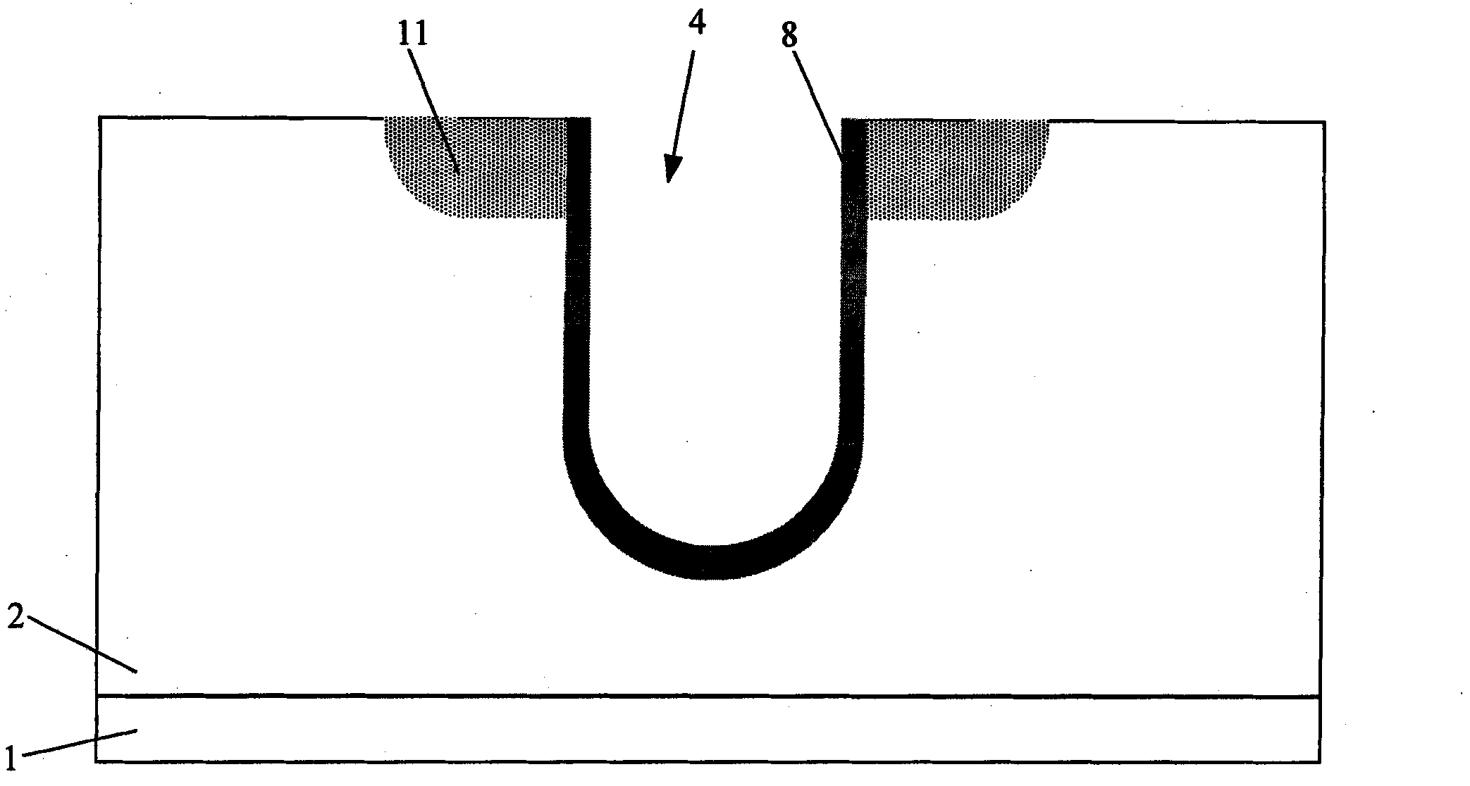
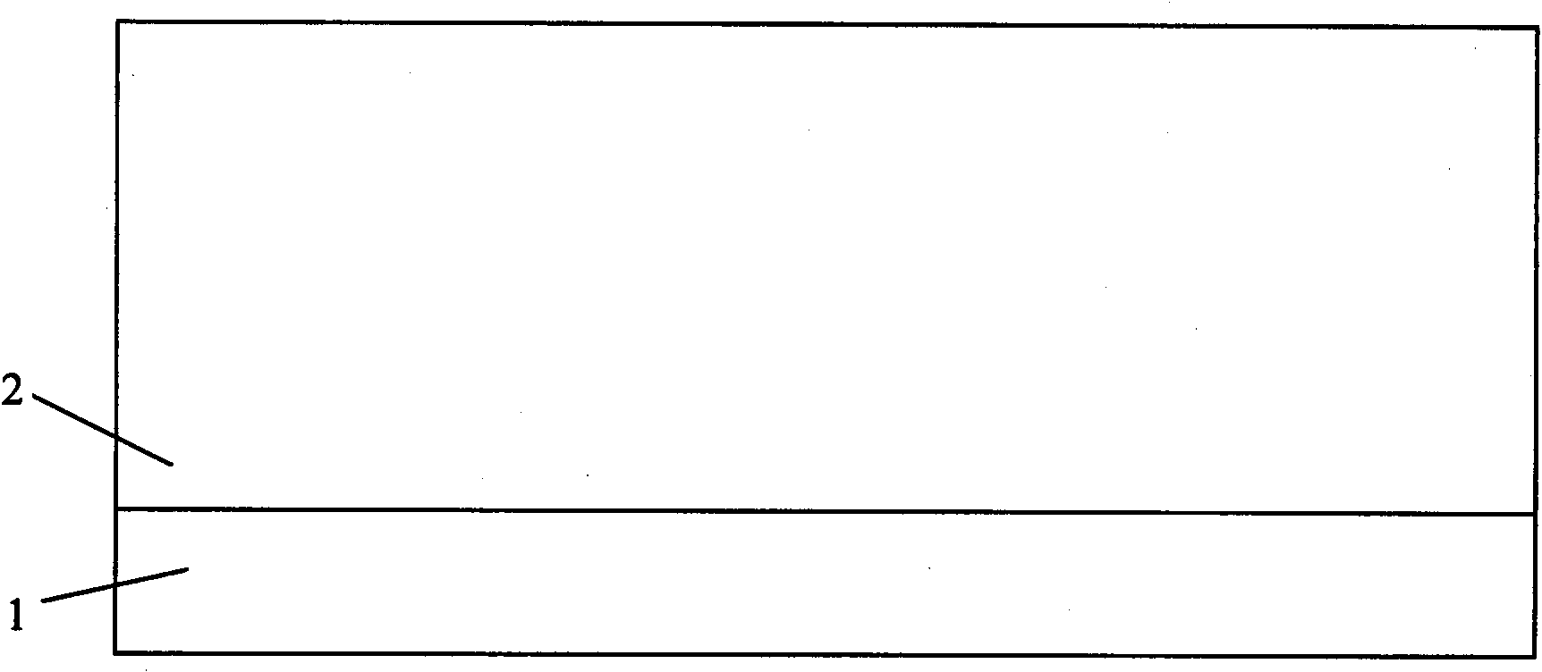
[0054] Step 1: Reference image 3 , Figure 4 , using an N+ type substrate doped with As, growing a 5-10um epitaxial layer 2 on the substrate, the preferred thickness of the epitaxial layer 2 is 3-3.5um, and using a thermal oxidation process on the epitaxial layer 2 Depositing a third oxide layer 3 of 6000A;

[0055] Step 2: Reference Figure 4-Figure 9 , etch a trench 4 with a width of 0.4-0.6um and a depth of 1um-1.6um and form a thickened oxide layer 6 with a thickness of 0.15-0.25um in the trench 4, wherein the thickened oxide layer is formed Step 6 also includes:

[0056] Step 20: Deposit a second oxide layer 5 in the trench until the trench 4 is completely filled. For details, refer to Figure 4 , Figure 5 and Figure 6 , coat 2um photoresist 3a on the third oxide layer 3, form trench etching window 3b after exposu...

Embodiment 2

[0067] Such as Figure 3 to Figure 18 As shown, another embodiment of the present invention manufactures the trench power MOSFET and comprises the following process steps:

[0068] Steps 1-5 of the method in the second embodiment are the same as those in the first embodiment, except that the following steps are also included.

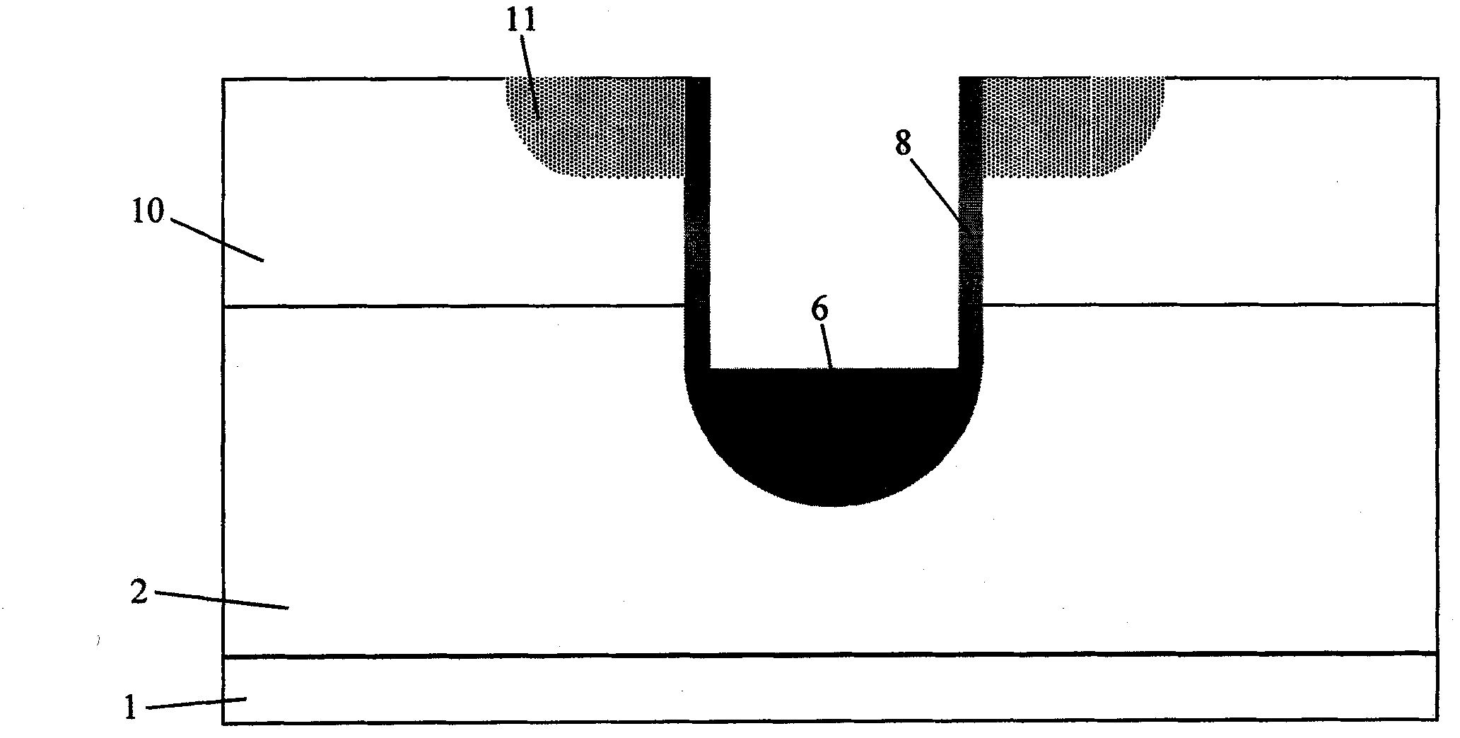
[0069] Step 6: Reference Figure 15 , Figure 16 , deposit a first oxide layer 12 with a thickness of 1.6-1.7um, and grind the first oxide layer 12 by chemical mechanical polishing, and the thickness of the first oxide layer 12 after grinding is 6000-8000A, and then contact Hole photolithography is used to carve a contact hole window 13, and a grooved contact hole 14 is formed through the contact hole window 13 using a plasma etching process, and the grooved contact hole 14 passes through the first oxide layer 12, the source region 11 and is connected with The P well region 10 is contacted, and the groove contact hole 14 has a width of 0.3-0.4um and ...

Embodiment 3

[0085] Embodiment 2 uses a P-type semiconductor, its principle is the same as Embodiment 1 and Embodiment 2, and the process steps are also the same as Embodiment 1. The difference is that the substrate it uses is a P-type substrate, on which the substrate grows The epitaxial layer is a P-type epitaxial layer, the well above the epitaxial layer is an N-well region, the source region above the N-well region is a P+-type source region, and there is P+-doped polysilicon in the trench. The implanted region is an N+ implanted region, and the rest of the oxide layer and the filling metal in the trench contact hole are the same as those in Embodiment 1 and Embodiment 2.


PUM

PropertyMeasurementUnit
Thicknessaaaaaaaaaa
Thicknessaaaaaaaaaa
Thicknessaaaaaaaaaa

Abstract

The invention discloses a groove type power MOSFET (Metal-Oxide-Semiconductor Field Effect Transistor) comprising an N type substrate, an N type epitaxial layer, a P well region, a source region, a first oxidization layer and a P+ injection zone, wherein the N type epitaxial layer is grown on the substrate; the P well region is formed on the epitaxial layer; the source region is arranged above the P well region; the first oxidization layer covers the source region; and the P+ injection zone is positioned in the P well region under the source region. The groove type power MOSFET is characterized by also comprising a plurality of grooves which pass through the source region and the P well region and contact with the epitaxial layer, wherein the bottoms of the grooves are provided with thickened oxidization layers with the thickness of 0.15-0.25 mum. The invention also provides a manufacturing method of the groove type power MOSFET. The grid-drain capacitance of the MOSFET is reduced under the condition that the starting voltage of the MOSEFT is not influenced, and thereby, the switching speed of the groove type power MOSFET is improved.

Description

technical field [0001] The invention relates to a structure of a trench power MOSFET and a manufacturing method thereof. Background technique [0002] At present, power MOSFET (Metal Oxide Semiconductor Field Effect Transistor, Metal Oxide Semiconductor Field Effect Transistor) has been widely used in various electronic and communication products, especially some switching power supply circuits, which are characterized by low power consumption and fast speed. The trench power MOSFET has a lower on-resistance under the same area as the common horizontal MOSFET because its conduction channel is in the vertical direction. [0003] In the application of switching power supply, the magnitude of the gate charge of the power MOSFET directly affects the switching frequency, and the MOSFET with low gate charge will bring higher switching efficiency. Although the on-resistance of the trench power MOSFET is smaller than that of the ordinary lateral MOSFET, due to the limitation of the...

Claims


Application Information

Patent Timeline
IPC IPC(8): H01L27/088H01L29/78H01L29/06H01L29/51H01L21/8234H01L21/336
CPCH01L29/41766H01L29/66734H01L29/456H01L29/66727H01L29/1095H01L29/42368H01L29/7813
Inventor 纪刚顾建平倪凯彬钟添兵
Owner WILL SEMICON (SHANGHAI) CO LTD
Why Eureka
Try Eureka