Production method of MOS (Metal Oxide Semiconductor) transistor

A technology of a MOS transistor and a manufacturing method, which is applied to the manufacturing field of MOS transistors and can solve the problems of difficulty in forming an ultra-shallow junction, difficulty in lateral diffusion, and the like

Active Publication Date: 2010-12-29
SEMICON MFG INT (SHANGHAI) CORP
View PDF3 Cites 6 Cited by
  • Summary
  • Abstract
  • Description
  • Claims
  • Application Information

AI Technical Summary

Problems solved by technology

[0010] In the above-mentioned method of forming a MOS transistor, in order to prevent overrun between the source and the drain and to suppress the short channel effect, the implantation of the source/drain is divided into two steps, that is, low-doped drain implantation and heavily doped source/drain implants

Method used


Image

  • Production method of MOS (Metal Oxide Semiconductor) transistor
  • Production method of MOS (Metal Oxide Semiconductor) transistor
  • Production method of MOS (Metal Oxide Semiconductor) transistor

Examples


Embodiment Construction

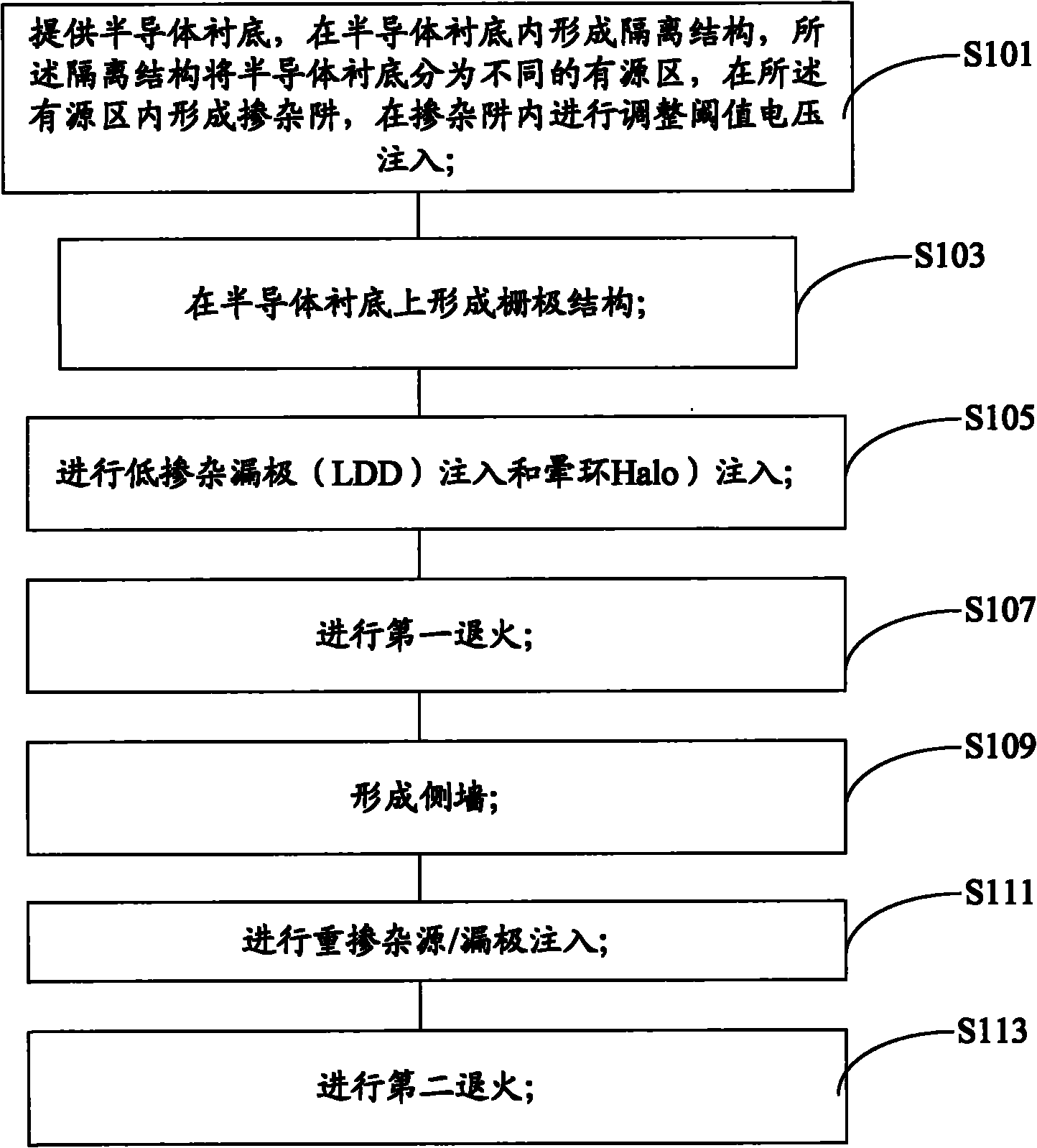
[0028] As mentioned above, based on the above experimental research and theoretical derivation, the inventors of the present invention found that the LDD implanted region in the prior art needs to undergo at least two anneals, making it difficult to form an ultra-shallow junction and to control lateral diffusion. Based on the above findings, the inventors of the present invention annealed the LDD implanted region only once by changing the process, and improved the annealing process to reduce the diffusion of the LDD implanted ions in the depth direction. The technology reduces the dose or energy of LDD implantation to form a shallow junction, so it can prevent the ion diffusion area of ​​the LDD implantation region from being too large, which is conducive to the formation of an ultra-shallow junction; at the same time, because the implantation energy and dose are not reduced, the relatively small area of ​​the LDD implantation region can be maintained. Low resistance, high drai...


PUM


Abstract

The invention relates to a production method of an MOS (Metal Oxide Semiconductor) transistor, which comprises the following steps of: carrying out etching on a first medium layer and a polysilicon layer for the first time to form an auxiliary hard mask layer; oxidizing the polysilicon layer in the auxiliary hard mask layer to form a first oxide layer; injecting for the first time to form high doping source/drain electrodes; removing the first oxide layer; etching the auxiliary hard mask layer to form a polysilicon gate electrode and a gate medium layer; oxidizing the polysilicon gate electrode for the second time to form a second oxide layer; forming first side walls on a semiconductor substrate and two sides of the polysilicon grate electrode; injecting for the second time to form low doping source/drain electrodes and then forming a second medium layer; and annealing. By adjusting the process of the MOS transistor, the high doping source/drain electrodes are formed before the low doping source/drain electrodes are formed, and the high doping source/drain electrodes and the low doping source/drain electrodes are only annealed once, and over-large diffusion area can not be caused by long-time annealing, thereby facilitating the form of ultra shallow junctions.

Description

technical field [0001] The invention relates to the technical field of semiconductors, in particular to a manufacturing method of a MOS transistor. Background technique [0002] As the semiconductor industry moves toward smaller and faster devices, the feature lateral dimensions and depths of semiconductor devices are gradually decreasing, and the requirements for device performance are getting higher and higher. [0003] US Patent No. US6512273 discloses a manufacturing method for MOS transistors, by forming polysilicon sidewalls for n-channel transistors and forming silicon nitride sidewalls for p-channel transistors, thereby optimizing the performance of each device. Driving current to improve hot-carrier lifetime of n-channel devices. [0004] The US patent No. US5869379 discloses a method of manufacturing a MOS transistor, which reduces the lateral coupling capacitance between adjacent gate electrodes by forming air spacers on both sides of the polysilicon gate electro...

Claims


Application Information

Patent Timeline
IPC IPC(8): H01L21/336H01L21/28H01L21/265
Inventor 赵猛
Owner SEMICON MFG INT (SHANGHAI) CORP
Why Eureka
Try Eureka