Bottom source nmos triggered zener clamp for configuring an ultra-low voltage transient voltage suppressor (tvs)
A technology of transient voltage suppression and oxide semiconductors, which is applied in the production of transient voltage suppressors and improved circuit structures, and can solve problems affecting the response time of transient voltage suppressor circuits.
- Summary
- Abstract
- Description
- Claims
- Application Information
AI Technical Summary
Problems solved by technology
Method used
Image

Examples
Embodiment Construction
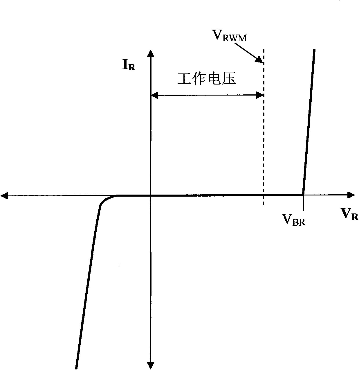
[0037] Figure 4A and Figure 4B Respectively represent the cross-sectional view of the transient voltage suppressor 100 of the present invention and the corresponding equivalent circuit diagram. Figure 4C is a current-voltage graph showing the current conduction and voltage characteristics of the transient voltage suppressor 100 . The transient voltage suppressor device 100 is formed in an N+ substrate 105 with an N- epitaxial layer 110 above the substrate, an anode terminal 115 is arranged on the bottom of the substrate, a cathode terminal 120 is arranged on the top surface of the substrate, and the substrate and the N+ drain The pole / collector region 130 is in contact. As shown in the equivalent circuit 100 , the device includes an NMOSFET 160 and an NPN bipolar transistor 170 in addition to the transient voltage suppressor diode 150 . The connection mode of the terminals of the NMOS 160 and the NPN bipolar transistor 170 in this structure will be described below. The ...
PUM
 Abstract
Description
Claims
Application Information
 - R&D
- Intellectual Property
- Life Sciences
- Materials
- Tech Scout
- Unparalleled Data Quality
- Higher Quality Content
- 60% Fewer Hallucinations
Browse by: Latest US Patents, China's latest patents, Technical Efficacy Thesaurus, Application Domain, Technology Topic, Popular Technical Reports.
© 2025 PatSnap. All rights reserved.Legal|Privacy policy|Modern Slavery Act Transparency Statement|Sitemap|About US| Contact US: help@patsnap.com