Power metal oxide semiconductor field effect transistor (MOSFET) device with tungsten spacing layer in contact hole and preparation method thereof

A manufacturing method and contact hole technology, applied in semiconductor/solid-state device manufacturing, semiconductor devices, electric solid-state devices, etc., can solve problems such as poor step coverage, aluminum puncture, small contact hole size, etc., to avoid leakage short circuit, ensure The effect of product quality

Active Publication Date: 2012-07-04
ALPHA & OMEGA SEMICON INC
View PDF0 Cites 0 Cited by
  • Summary
  • Abstract
  • Description
  • Claims
  • Application Information

AI Technical Summary

Problems solved by technology

[0006] However, another problem caused by this process is that if there is a pit at the bottom corner of the contact hole 7', the Ti / TiN barrier layer 8' will not be able to achieve good step coverage to prevent silicon and direct contact with aluminum, aluminum piercing still occurs at the bottom corner 71' of the contact hole 7'
[0007] Due to the current advanced semiconductor manufacturing technology, the integration of semiconductor devices can be improved by reducing the external dimensions of the devices; for example, the wall-to-wall pitch size (wall-to-wall pitch size) in some currently used MOSFETs is about 1 micron, resulting in a smaller contact hole size and a shallower source / body region depth
Thus, the poorer step coverage of the Ti / TiN barrier layer will lead to more Al piercing due to pits at the bottom corners of the contact holes

Method used


Image

  • Power metal oxide semiconductor field effect transistor (MOSFET) device with tungsten spacing layer in contact hole and preparation method thereof
  • Power metal oxide semiconductor field effect transistor (MOSFET) device with tungsten spacing layer in contact hole and preparation method thereof
  • Power metal oxide semiconductor field effect transistor (MOSFET) device with tungsten spacing layer in contact hole and preparation method thereof

Examples


Embodiment Construction

[0062] The following combination image 3 , Figure 4 , Figure 5 and Figures 6A-6E , the specific implementation of the present invention will be described in detail through several examples.

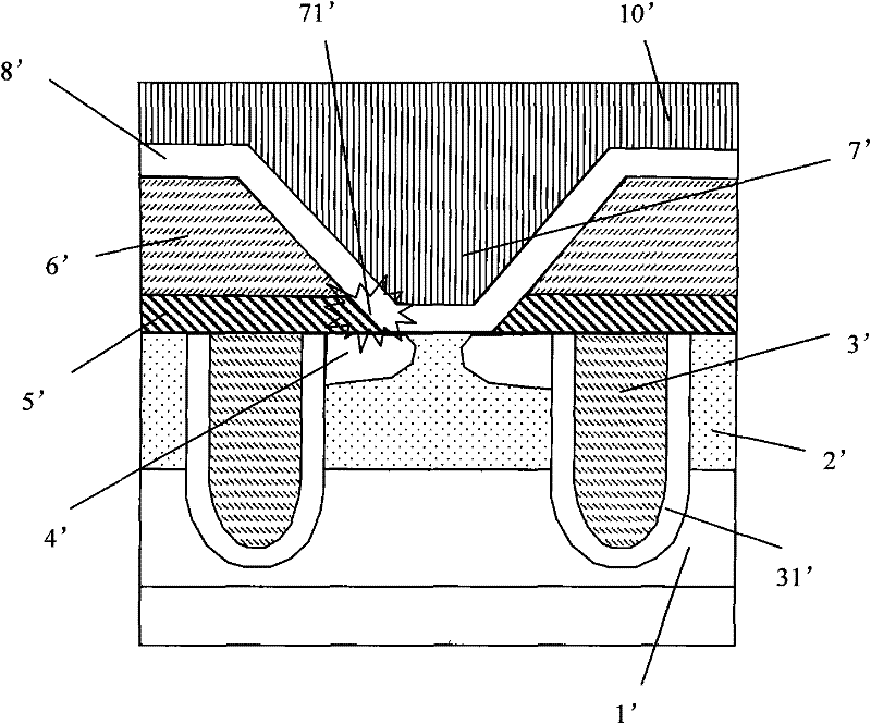
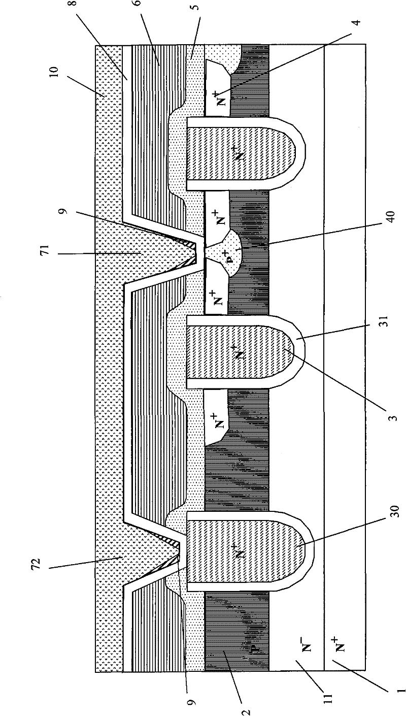
[0063] Such as image 3 Shown is a cross-sectional view of an embodiment of the power MOSFET device with tungsten sidewalls in the contact hole according to the present invention. The power MOSFET device is an N channel semiconductor device, which includes an N+ highly doped bottom substrate 1 as a drain, and an N- epitaxial layer 11 is grown on the N+ bottom substrate 1; on the N- epitaxial layer 11 A P-body region 2 is formed thereon. In the P-body region 2, there are several grooves penetrating the P-body region 2 and extending to a certain depth in the N-epitaxial layer 11, and filling the grooves with conductive material such as polysilicon to form the grooves Gate 3, and a thinner gate insulating layer 31 formed along the sidewall and bottom of the trench is also arranged ...


PUM


Abstract

The invention provides a power metal oxide semiconductor field effect transistor (MOSFET) device with a tungsten spacing layer in a contact hole and a preparation method thereof. The power MOSFET device is characterized by comprising a groove grid electrode and the tungsten spacing layer, wherein the groove grid electrode is isolated in a groove and is contacted with a source electrode / body region formed in the contact hole; and the tungsten spacing layer is deposited at the bottom corner of the contact hole and arranged between a Ti / TiN barrier layer and an aluminium metal layer so as to cover the bottom corner of the contact hole. The tungsten spacing layer is arranged at the bottom corner of the contact hole, so the aluminium puncturing problem caused by direct contact of the silicon and the aluminium resulted from the formation of a pit at the bottom corner of the contact hole and the Ti / TiN barrier layer does not have high step coverage can be effectively prevented, the failure of the power MOSFET device from Idss leakage and short circuit is further avoided, and the product quality of the device is guaranteed.

Description

technical field [0001] The invention belongs to the field of semiconductor wafer manufacturing, and in particular relates to a power MOSFET (metal oxide semiconductor field effect transistor) device with a tungsten spacer layer arranged in a contact hole and a manufacturing method thereof. Background technique [0002] Such as figure 1 Shown is a schematic structural diagram of a power MOSFET device in the prior art. The MOSFET device has a bottom substrate 1' serving as a drain; a body region 2' is formed on the bottom substrate 1'. A plurality of trenches penetrating through the body region 2' and extending to a certain depth in the substrate 1' are opened in the body region 2', trench gates 3' are arranged in the trenches, and A thinner gate insulating layer 31 ′ formed along the sidewall and bottom of the trench is also provided in the trench, which is used to insulate the trench gate 3 ′ from the substrate 1 ′ and the body region 2 ′. In said body region 2' and around...

Claims


Application Information

Patent Timeline
Patent Type & Authority Patents(China)
IPC IPC(8): H01L27/088H01L23/532H01L21/8234H01L21/768
CPCH01L2924/0002
Inventor 何增谊隋晓明王健沈思杰
Owner ALPHA & OMEGA SEMICON INC
Why Eureka
Try Eureka