Method for building optical proximity correction model, optical proximity correction method and mask

A technology for optical proximity correction and reticle, which is applied in the fields of optics, photo-engraving process of pattern surface, originals for opto-mechanical processing, etc. Improve chip performance and product yield, accurate optical proximity correction

Active Publication Date: 2011-01-05
SEMICON MFG INT (SHANGHAI) CORP +1
View PDF2 Cites 22 Cited by
  • Summary
  • Abstract
  • Description
  • Claims
  • Application Information

AI Technical Summary

Problems solved by technology

However, it can be seen that there is a large space redundancy between the new figure formed by the chamfer 204 and the actual figure formed by the arc 202, which will affect the parameters such as key dimensions and spatial periods of the figure; in addition , in the actual processing of the stepping lithography machine, it does not follow a straight line, but disassembles the oblique line into multiple broken lines connected head to tail according to the resolution, and steps one by one according to the broken lines. The above technical solution greatly increases The amount of data that needs to be calculated and processed affects production efficiency

Method used


Image

  • Method for building optical proximity correction model, optical proximity correction method and mask
  • Method for building optical proximity correction model, optical proximity correction method and mask
  • Method for building optical proximity correction model, optical proximity correction method and mask

Examples


Embodiment Construction

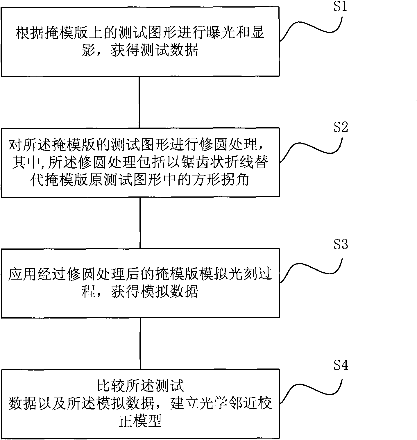
[0027] In model-based OPC, it is very important to accurately establish an optical proximity correction model that conforms to the actual exposure situation. Generally speaking, a test reticle can be used for exposure first, and the test data can be obtained by measuring the size of the exposure pattern obtained on the silicon wafer after the actual exposure; then the photolithography process can be simulated according to the test pattern on the test reticle used , obtain simulated data by measuring the size of the simulated result; then, compare the test data and simulated data to establish an optical proximity correction model, so that when the optical proximity correction model is applied to the simulated data, it is possible to obtain data same result.

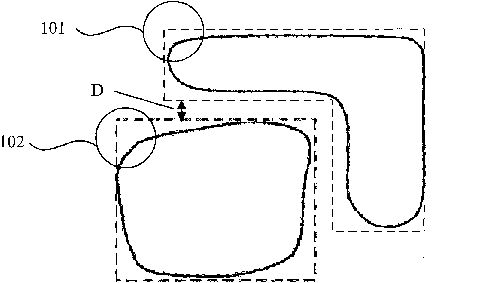
[0028] In actual lithography, when the test pattern on the mask plate is transferred to the photoresist layer through exposure and development steps, the pattern will appear square corners become rounded after development,...


PUM


Abstract

The invention relates to a method for building an optical proximity correction model, an optical proximity correction method and a mask. The method for building the optical proximity correction model comprises the following steps of: exposing and developing according to a test pattern on the mask to obtain test data; rounding the test pattern of the mask, wherein the rounding treatment comprises the replacement of square corners in the original test pattern in the mask with zigzag broken lines; simulating the photoetching process by using the rounded mask to obtain simulate data; comparing the test data with the simulated data, and building the optical proximity correction model. The zigzag broken lines are used for rounding the square corners, so that optical proximity correction becomesmore accurate; thus, the rate of finished products is increased, labor and time are saved, and production efficiency is improved.

Description

technical field [0001] The invention relates to an optical proximity correction technology, in particular to an optical proximity correction method suitable for corner rounding. Background technique [0002] With the development of integrated circuits, the design size is getting smaller and smaller. Due to the diffraction and interference of light, there are certain deformations and deviations between the photolithography pattern actually obtained on the silicon wafer and the mask pattern. During the photolithography process, the projection light passes through the mask plate and spreads to the materials of each layer of the silicon wafer, so that the photolithographic patterns related to the mask pattern are obtained on the materials of each layer of the silicon wafer. According to the principle of light wave diffraction and interference, light waves will diffract when passing through the mask, and light waves at different positions of the mask will also interfere. Therefor...

Claims


Application Information

Patent Timeline
Patent Type & Authority Applications(China)
IPC IPC(8): G03F1/14G03F1/36
Inventor 朴世镇
Owner SEMICON MFG INT (SHANGHAI) CORP
Why Eureka
Try Eureka