
Integrated microstrip circulator and preparation method thereof

A circulator and microstrip technology, applied in the electronic field, can solve problems such as large dielectric loss

Inactive Publication Date: 2013-01-09
UNIV OF ELECTRONICS SCI & TECH OF CHINA
View PDF4 Cites 0 Cited by
  • Summary
  • Abstract
  • Description
  • Claims
  • Application Information

AI Technical Summary

Problems solved by technology

However, experiments have shown that because polycarbonate templates are easy to react with chemical solutions, conventional photolithography methods cannot be used to prepare the metal pattern layer used in devices, that is, the Y junction. Microstrip circulator has high dielectric loss and is not compatible with microwave monolithic integrated circuit technology

Method used


Image

  • Integrated microstrip circulator and preparation method thereof
  • Integrated microstrip circulator and preparation method thereof

Examples


Embodiment approach 1

[0028] (1) adopting DC magnetron sputtering method to prepare 2 micron thick gold (Au) film on GaAs substrate;

[0029] (2) Utilize radio frequency magnetron sputtering method to prepare 40 micron thick aluminum film on gold film, the purity of aluminum target is 99.9%;

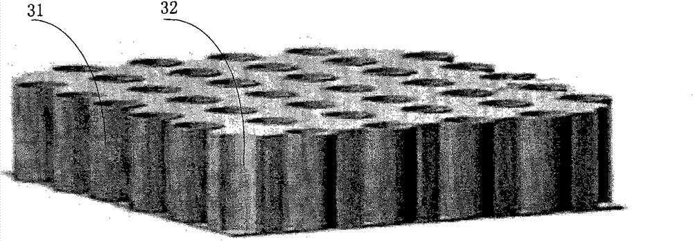
[0030] (3) the aluminum film that step (2) obtains is put into the H of 70g / L 3 PO 4 In the solution, under the working voltage of 30V and the temperature of 18°C, the first anodic oxidation treatment was performed for 0.5 hours; then the sample after the first oxidation treatment was placed in 70g / L H 3 PO 4 The solution was soaked for 0.5 hours; finally the sample was put into 70g / L H 3 PO 4 In the solution, under the working voltage of 30V and the temperature of 18°C, the first anodic oxidation treatment was performed for 1 hour. Its surface morphology is observed with a scanning electron microscope, and its average pore size is 50nm.

[0031](4) Electroplating elemental magnetic metal cobalt in the ...

Embodiment approach 2

[0038] Except that the secondary anodizing voltage in the step (3) is 45V, other steps are the same as the first embodiment.

Embodiment approach 3

[0040] Except that the secondary anodic oxidation voltage in step (4) is 60V, other steps are the same as that of Embodiment 1.

[0041] Table 1 Implementation Effects

[0042] Example

[0043] In Table 1, the volume reduction ratio and weight reduction ratio of the samples prepared in the three embodiments are compared with the existing separate assembly type circulator.


PUM

PropertyMeasurementUnit
thicknessaaaaaaaaaa
thicknessaaaaaaaaaa
pore sizeaaaaaaaaaa

Abstract

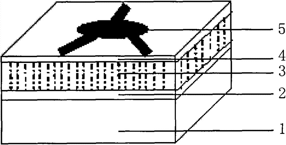
The invention provides an integrated microstrip circulator, belonging to the electronic technical field. The integrated microstrip circulator comprises a metal bottom electrode on a microwave medium substrate, a nanowire ferromagnetic composite medium, an insulating layer and a Y-junction of the microstrip circulator, wherein the nanowire ferromagnetic composite medium is compounded by a ferromagnetic metal nanowire and aluminum oxide, the aluminum oxide has a nanometer grade porous structure, and the ferromagnetic metal nanowire is filled in the nanometer pores of the aluminum oxide by the electroplating process. The preparation method comprises the following steps: depositing the metal bottom electrode and a metal aluminum film on the microwave medium substrate; performing secondary anode oxidizing treatment on the metal aluminum film; filling the ferromagnetic metal nanowire in the nanometer grade pores of the aluminum oxide by the electroplating process; and manufacturing the required Y junction for the circulator. In the method, the nanowire ferromagnetic composite medium compounded by the ferromagnetic metal and the porous aluminum oxide is adopted as an automatic biasing magnetic medium of the microstrip circulator, the work efficiency of the microstrip circulator can be improved, and the volume and the weight of the circulator can be reduced; and the preparation process of the microstrip circulator can be compatible with the microwave integration circuit process.

Description

technical field [0001] The invention belongs to the field of electronic technology, relates to microwave technology and microwave monolithic integrated circuits, in particular to an integrated microstrip magnetic circulator applicable to microwave integrated circuits and a preparation method thereof. Background technique [0002] The circulator is one of the essential devices in the microwave circuit system. It can be used as a shunt element in microwave communication; it can be used as a directional coupler and isolator in the test equipment; it can improve the gain bandwidth of the amplifier in the parametric amplifier ; Used as a duplexer in radar and microwave systems. [0003] From the perspective of the development trend of circulators, miniaturization, high frequency band, and ultra-wideband are the future development directions, so microstrip circulators have become the main object of current circulator research. As far as the microstrip circulator is concerned, to ...

Claims


Application Information

Patent Timeline
Patent Type & Authority Patents(China)
IPC IPC(8): H01P1/387H01P11/00
Inventor 钟智勇刘爽张怀武唐晓莉荆玉兰贾利军白飞明苏桦
Owner UNIV OF ELECTRONICS SCI & TECH OF CHINA
Learn More