Method for producing photoelectrochemical microfluidic detection chip of three-electrode system

A three-electrode system, photoelectrochemical technology, applied in the fields of material electrochemical variables, analytical materials, instruments, etc., can solve the problems of complex production process, high cost, and equipment time-consuming, etc., to improve catalytic efficiency, low production cost, Less time consuming effect

Inactive Publication Date: 2011-01-19
DONGHUA UNIV
View PDF5 Cites 13 Cited by
  • Summary
  • Abstract
  • Description
  • Claims
  • Application Information

AI Technical Summary

Problems solved by technology

However, the main disadvantages in the production of microfluidic chips are as follows: (1) high cost
Because the photolithography technology used in the microelectronics industry is usually used, making a microfluidic chip requires a lot of special equipment and takes a lot of time, and the manufacturing process is very complicated.
(2) The sealing of microfluidic chips is difficult
In the process of photolithography or micromachining, the surface of the substrate constituting the microreactor is usually damaged, resulting in unevenness, and the sealing effect with fixtures or adhesives is not good, and leakage is prone to occur

Method used


Image

  • Method for producing photoelectrochemical microfluidic detection chip of three-electrode system
  • Method for producing photoelectrochemical microfluidic detection chip of three-electrode system
  • Method for producing photoelectrochemical microfluidic detection chip of three-electrode system

Examples


Embodiment 1

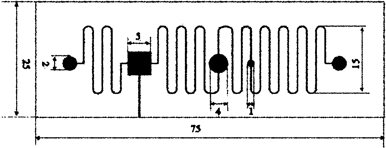
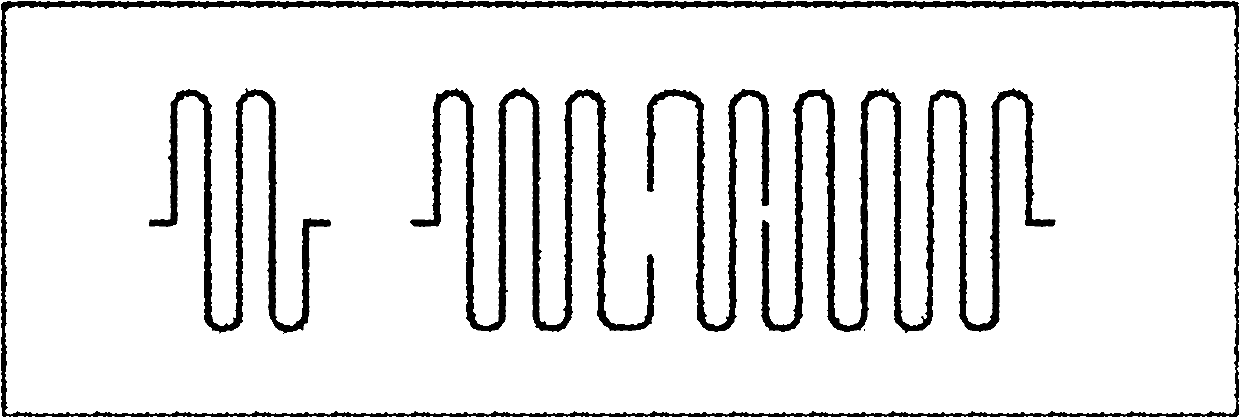
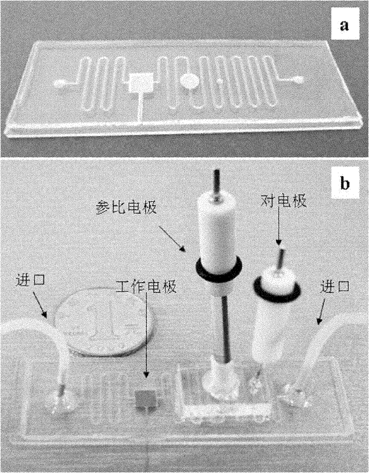
[0035] The liquid PDMS matrix and the curing agent are mixed uniformly in a mass ratio of 10:1. A glass sheet with a size of 25mm×75mm and a thickness of 1mm was adsorbed on the turntable of the homogenizer, the PDMS was poured on the glass sheet, and rotated at a speed of 1000 revolutions / min for 30 seconds. Then, the glass slide with PDMS was placed in an environment of 120°C for 6 minutes to cure the PDMS. Graphics designed according to the drawing such as figure 2 As shown, use CO 2 The laser engraves the channel on the PDMS. First sculpt as image 3 In the part shown, the laser power used is 12W, the engraving speed is 50cm / s, and the resulting channel has a depth of 0.2mm and a width of 0.2mm. Then engrave the remaining part, the laser power used is 15W, the engraving speed is 50cm / s, the depth of the resulting figure is 0.3mm, and the size is as figure 2 Shown. After the carving is completed, you get Figure 4 The substrate shown in a. Place the electrode covered wi...

Embodiment 2

[0038] The liquid PDMS matrix and the curing agent are mixed uniformly in a mass ratio of 10:1. A glass sheet with a size of 25mm×75mm and a thickness of 2mm was adsorbed on the turntable of the homogenizer, and the PDMS was poured on the glass sheet and rotated at 800 rpm for 45 seconds. Then, the glass slide loaded with PDMS was placed in an environment at 100°C for 10 minutes to cure the PDMS. Graphics designed according to the drawing such as figure 2 As shown, use CO 2 The laser engraves the channel on the PDMS. First sculpt as image 3 In the part shown, the laser power used is 15W, the engraving speed is 50cm / s, and the resulting channel has a depth of 0.3mm and a width of 0.5mm. Then engrave the remaining part, the laser power used is 15W, the engraving speed is 40cm / s, the depth of the resulting figure is 0.35mm, and the size is as figure 2 Shown. After the engraving is completed, the electrode covered with the nano-titanium dioxide active layer is placed in the wo...

Embodiment 3

[0040] The liquid PDMS matrix and the curing agent are mixed uniformly in a mass ratio of 10:1. A glass sheet with a size of 25mm×75mm and a thickness of 3mm was adsorbed on the turntable of the homogenizer, the PDMS was poured on the glass sheet, and rotated at 500 rpm for 60 seconds. Then, the glass slide loaded with PDMS was placed in an environment at 150°C for 3 minutes to cure the PDMS. Graphics designed according to the drawing such as figure 2 As shown, use CO 2 The laser engraves the channel on the PDMS. First sculpt as image 3 In the part shown, the laser power used is 20W, the engraving speed is 70cm / s, the resulting channel depth is 0.4mm, and the width is 1mm. Then engrave the remaining part, the laser power used is 20W, the engraving speed is 50cm / s, the depth of the resulting figure is 0.5mm, and the size is as figure 2 Shown. After the engraving is completed, the electrode covered with the nano-titanium dioxide active layer is placed in the working electrod...


PUM

PropertyMeasurementUnit
thicknessaaaaaaaaaa
depthaaaaaaaaaa
widthaaaaaaaaaa

Abstract

The invention relates to a method for producing a photoelectrochemical microfluidic detection chip of a three-electrode system. The method comprises the following steps: coating liquid polydimethylsiloxane (PDMS) on a glass sheet and curing the PDMS to form a substrate; forming a micro-channel and corresponding work electrode pool, reference electrode pool, counter electrode pool and import/export pool from a pre-designed pattern on the PDMS by using a laser engraving method; placing the work electrodes and connecting with leads; sealing another non-etched PDMS as a cover plate by oxygen plasma processing; and finally integrating the reference electrodes and the counter electrodes to produce the photoelectrochemical microfluidic detection chip of the three-electrode system. The production method is easy to operate; the size of the micro-channel is controllable; the sealing of the microfluidic chip is realized without additional adhesive; after the sealing, the bonding is firm without leakage; and the method is applicable to photoelectrochemical detection and has the advantages of little oxygen consumption, fast detection and high flexibility.

Description

Technical field [0001] The invention belongs to the manufacturing field of microfluidic detection chips, and particularly relates to a method for manufacturing a three-electrode system photoelectrochemical microfluidic detection chip. Background technique [0002] The microfluidic chip analysis and test system is the development frontier of the Miniaturized Total Analysis Systems (μTAS) that appeared in the 1990s, and its development direction is to be more miniaturized, automated, rapid and portable. The basic feature of the microfluidic chip is the flexible combination and large-scale integration of multiple unit technologies on an overall controllable tiny platform. The advantage of this is that the sample processing time is greatly shortened, the detection resolution / sensitivity is significantly improved, and the consumption and cost are greatly reduced. The more far-reaching significance is that it is very likely to make the overall device of the microfluidic chip miniaturi...

Claims


Application Information

Patent Timeline
Patent Type & Authority Applications(China)
IPC IPC(8): G01N35/00G01N27/30
Inventor 王宏志穆庆辉李耀刚张青红
Owner DONGHUA UNIV
Why Eureka
Try Eureka