Structure of P-type GaN layer of GaN-based light-emitting diode chip

A technology of dies and holes, applied in semiconductor devices, electrical components, circuits, etc., can solve the problems of implanting plasmonic systems and limited distance of coupling enhancement effects

Active Publication Date: 2011-01-19
SHANDONG UNIV
View PDF4 Cites 35 Cited by
  • Summary
  • Abstract
  • Description
  • Claims
  • Application Information

AI Technical Summary

Problems solved by technology

[0005] The present invention aims at the problems of the existing SPP coupling enhanced radiation technology in the application of GaN-based LED devices to the problems of the implanted plasmon system and the limited distance of the coupling enhancement effect, and provides a method that can effectively utilize SPP coupled enhanced radiation to improve GaN-based LED light emission. Efficient GaN-based LED Die P-type GaN Layer Structure

Method used


Image

  • Structure of P-type GaN layer of GaN-based light-emitting diode chip
  • Structure of P-type GaN layer of GaN-based light-emitting diode chip
  • Structure of P-type GaN layer of GaN-based light-emitting diode chip

Examples


Embodiment 1

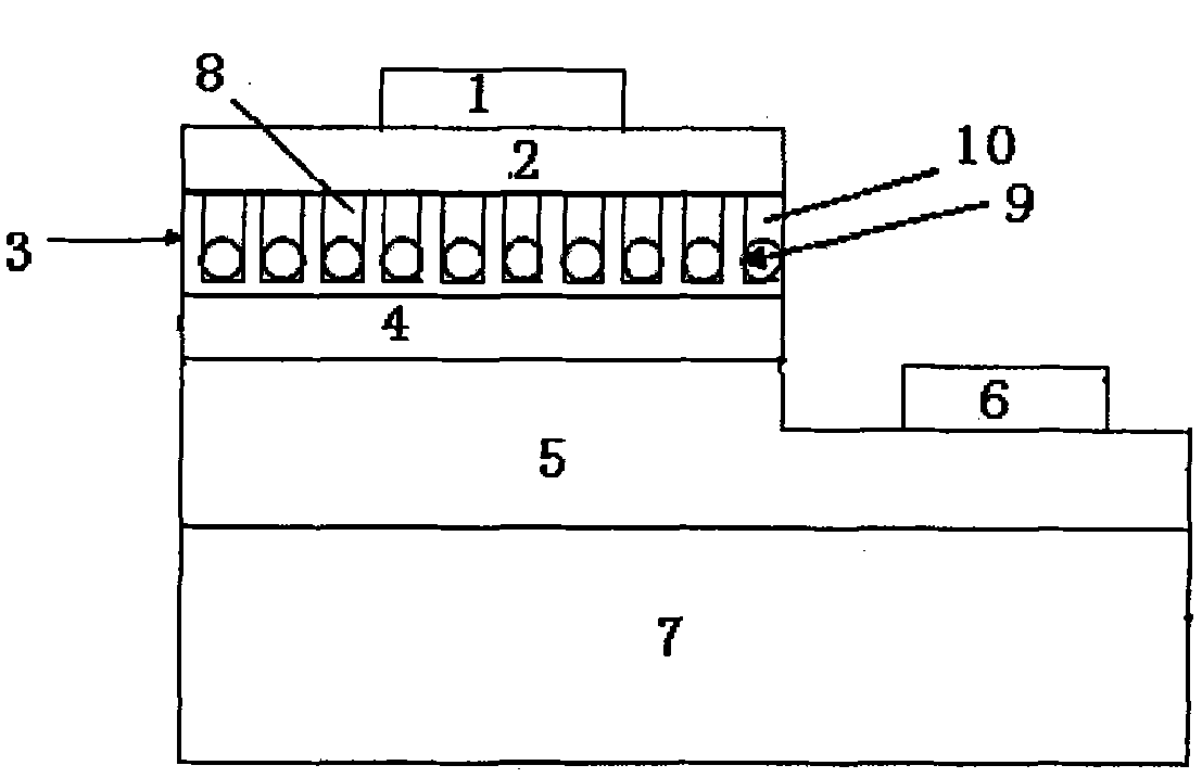
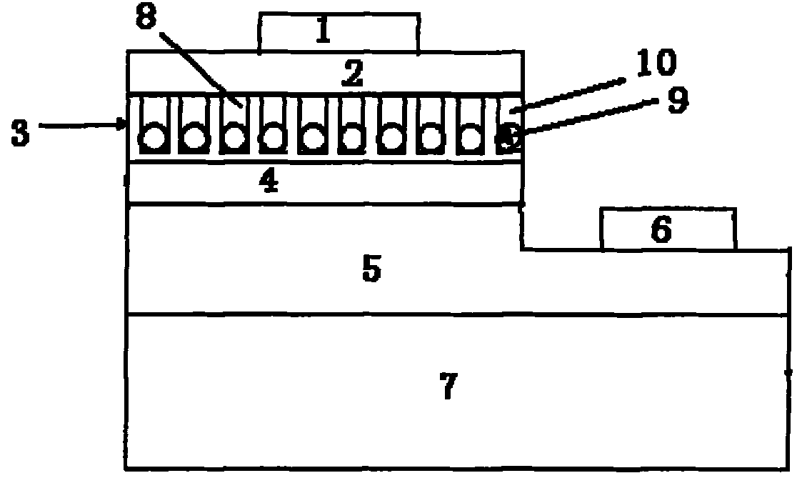
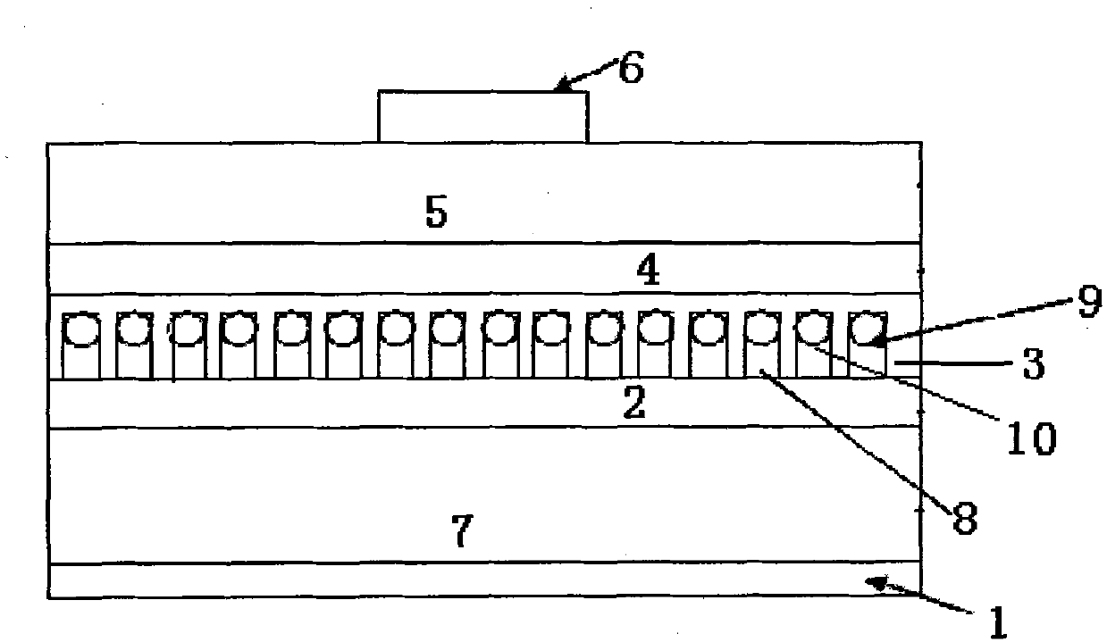
[0018] The structure of the P-type GaN layer on the conventional GaN-based LED tube core of the present invention, such as figure 1 shown. The die structure of a conventional GaN-based LED includes a P electrode 1, a P surface contact current spreading layer 2, a P-GaN layer 3, a quantum well active region 4, an N-GaN layer 5, an N electrode 6 and a substrate from top to bottom. Bottom 7. In the present invention, holes 8 with a diameter of 50 nanometers to 1000 nanometers are arranged on the P-GaN layer 3, and the distance between the holes is 0.1 micrometers to 10 micrometers. The distance between the bottom of the hole 8 and the quantum well active region 4 adjacent to the P-GaN layer 3 is 10 nanometers to 100 nanometers. The holes 8 are filled with metal particles 9 with a thickness of 10 nm to 400 nm, and the particle diameter of the metal particles 9 is 5 nm to 100 nm. The metal particles 9 are metal particles such as metal Ag, Al, Ni or Au, which can be obtained by t...

Embodiment 2

[0021] This embodiment is applied to a GaN-based LED tube core structure with a vertical flip-chip structure, such as figure 2 shown. The structure of the P-GaN layer on it is the same as that of the P-type GaN layer on the conventional GaN-based LED tube core in Example 1. The epitaxial layer is transferred to other substrates by flip-chip technology, and a high-power vertical structure chip can be produced. .


PUM

PropertyMeasurementUnit
diameteraaaaaaaaaa
particle diameteraaaaaaaaaa
thicknessaaaaaaaaaa

Abstract

The invention provides a structure of a P-type GaN layer of a GaN-based light-emitting diode (LED) chip, wherein the P-type GaN layer is provided with pores, the distance from the bottoms of pores to the quantum-well active area of the LED chip is 10-100nm, metal particles are filled in the pores, and transparent dielectric films are filled at the pore openings to block the metal particles. The P-type GaN layer of the invention is provided with nano-pores, each pore is provided with a metal particle; the metal particle-active layer dielectric heterostructure is transplanted at the nanoscale to form the dielectric heterostructure coupled by the nanometer metal particles and the quantum-well active area; and the coupling of the surface plasmon polariton (SPP) and excitons increases the luminous efficiency of the GaN-based LED.

Description

technical field [0001] The invention relates to a tube core structure of a GaN-based LED (light emitting diode), belonging to the technical field of optoelectronic devices. Background technique [0002] The core structure of a GaN-based LED generally includes a P electrode, a P surface contact current spreading layer, a P-GaN layer, a quantum well active region, an N-GaN layer, an N electrode, and a substrate from top to bottom. The structure causes the LED to have the problem of low radiation efficiency. How to improve the internal quantum efficiency and light extraction efficiency of LEDs, and enhance light radiation has become a hot spot in the technical competition of LED products. At present, research on LED technology often focuses on optimizing quantum well structure design, improving epitaxial film growth quality, and adopting new tube core technology to improve light extraction efficiency. Most of the most basic composite light-emitting principles of semiconductor ...

Claims


Application Information

Patent Timeline
Patent Type & Authority Applications(China)
IPC IPC(8): H01L33/02
Inventor 徐现刚沈燕胡小波
Owner SHANDONG UNIV
Why Eureka
Try Eureka