Plating structure and method for manufacturing electric material
A coating and structure technology, applied in chemical instruments and methods, circuits, thin material processing, etc., can solve the problems of reduced reflectivity, increased contact resistance, loss of silver luster and reflective performance, etc. The effect of low resistance
- Summary
- Abstract
- Description
- Claims
- Application Information
AI Technical Summary
Problems solved by technology
Method used
Image
Examples
experiment example
[0081] basic sample
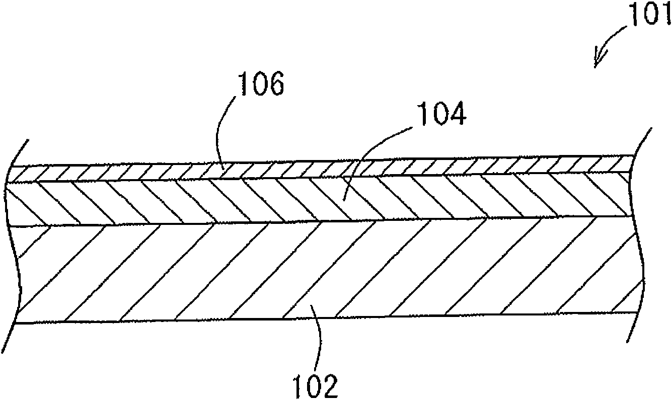
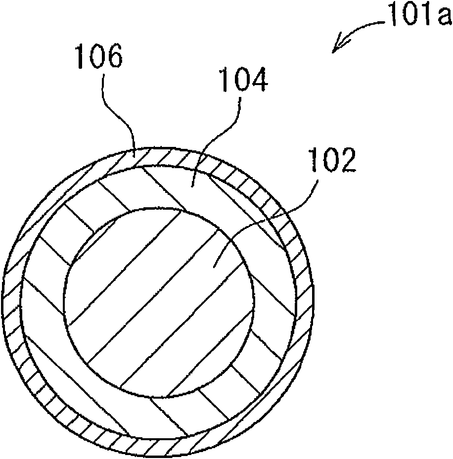
[0082] As a substance corresponding to the plating substrate 102 in FIG. 1 , a 1 cm square sheet of a copper alloy strip for lead frame (manufactured by Furukawa Electric Co., Ltd.: product name EFTEC3) was used. One surface of this sheet was plated with a 1 μm copper substrate, and then plated with 2 μm thick silver, which was used as a basic sample, and the basic sample was tin-plated and heat-treated according to the following experimental standards.
[0083] Experimental sample standard
[0084] L-1: Blank (in the state of the basic sample)
[0085] L-2: A tin layer with a thickness of 0.01 μm was formed on the silver surface of the basic sample by thin plating.
[0086] L-3: After forming a tin layer with a thickness of 0.01 μm on the silver surface of the basic sample by thin plating, the sample was heat-treated at 300° C. for 10 seconds.
[0087] L-4: A tin layer with a thickness of 0.02 μm was formed on the silver surface of the basic sampl...
Embodiment 1
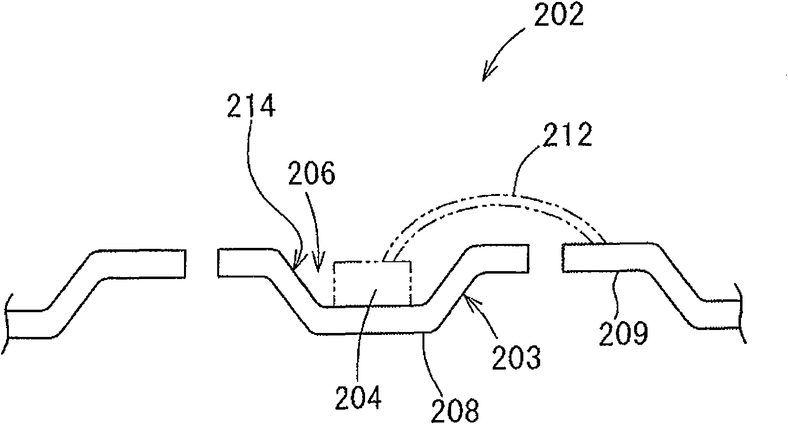
[0131] right figure 2 The frame shown in the shape of the substrate 203 is silver plated and tin plated. A copper alloy strip for a lead frame (manufactured by Furukawa Electric Co., Ltd.: EFTEC3) was used as a material for the frame of the base, and was formed by punching. After the degreasing treatment, the frame was acid-washed with 5% sulfuric acid, and the copper substrate was plated with a lustrous copper sulfate bath (copper sulfate 200g / L, sulfuric acid 50g / L, commercially available brightener 2mL / L). The film thickness of the base copper plating was 1.0 μm. Next, bright silver plating with a film thickness of 2 μm was performed using a glossy silver cyanide bath (35 g / L of silver cyanide, 90 g / L of potassium cyanide, and 10 g / L of potassium carbonate). Furthermore, tin with a film thickness of 0.01 μm was plated with an alkanolsulfonic acid bath (18 g / L of stannous, 100 g / L of free acid, and 10 mL / L of semi-brightener), followed by heat treatment at 250° C. for 10 ...
Embodiment 2
[0133] A stainless steel (SUS 304) plate with a thickness of 1 mm and a square of 1 cm is used as a substrate, and after degreasing treatment, it is acid-washed with 5% sulfuric acid, and a glossy copper sulfate bath (copper sulfate 200g / L, sulfuric acid 50g / L, commercially available brightener 2mL) / L) plated copper substrate. The film thickness of the base copper plating was 1.0 μm. Next, bright silver plating with a film thickness of 2 μm was performed using a glossy silver cyanide bath (35 g / L of silver cyanide, 90 g / L of potassium cyanide, and 10 g / L of potassium carbonate). Furthermore, tin with a film thickness of 0.01 μm was plated with an alkanolsulfonic acid bath (18 g / L stannous, 100 g / L free acid, 10 mL / L semi-brightener), and then heat-treated at 500° C. for 10 seconds to obtain a glossy plate . The vulcanization test was carried out, and the same result as L-3 in Table 1 was obtained.
PUM
| Property | Measurement | Unit |
|---|---|---|
| thickness | aaaaa | aaaaa |
| particle size | aaaaa | aaaaa |
| thickness | aaaaa | aaaaa |
Abstract
Description
Claims
Application Information
 - R&D
- Intellectual Property
- Life Sciences
- Materials
- Tech Scout
- Unparalleled Data Quality
- Higher Quality Content
- 60% Fewer Hallucinations
Browse by: Latest US Patents, China's latest patents, Technical Efficacy Thesaurus, Application Domain, Technology Topic, Popular Technical Reports.
© 2025 PatSnap. All rights reserved.Legal|Privacy policy|Modern Slavery Act Transparency Statement|Sitemap|About US| Contact US: help@patsnap.com


