Substrate for an organic light-emitting device, and organic light-emitting device incorporating it

A technology of organic light-emitting devices and substrates, which is applied in organic semiconductor devices, electric solid-state devices, semiconductor devices, etc., can solve the problems of expensive and complicated photolithography methods, and achieve the effect of improving and satisfying the conductivity

Inactive Publication Date: 2011-01-26
SAINT-GOBAIN GLASS FRANCE
View PDF9 Cites 12 Cited by
  • Summary
  • Abstract
  • Description
  • Claims
  • Application Information

AI Technical Summary

Problems solved by technology

And, in order to do this, especially expensive and complex photolithographic methods and passivation techniques are used

Method used


Image

  • Substrate for an organic light-emitting device, and organic light-emitting device incorporating it
  • Substrate for an organic light-emitting device, and organic light-emitting device incorporating it
  • Substrate for an organic light-emitting device, and organic light-emitting device incorporating it

Examples


Embodiment Construction

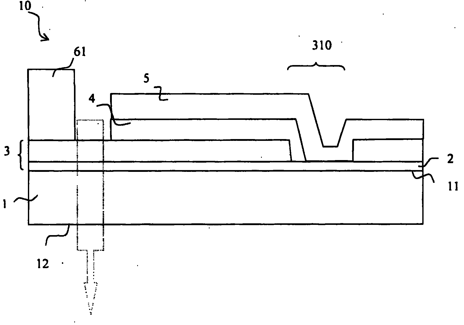
[0262] figure 1 is highly illustrative. It shows an organic light-emitting device 10 in cross-section (emitting through a substrate or "bottom emitting"), comprising in succession:

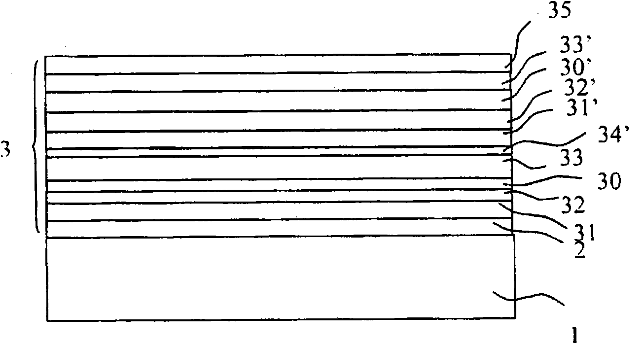
[0263] - a flat substrate 1 of optionally transparent or extra-transparent soda-lime-silica glass, for example starting from 0.7 mm in thickness, with a first and a second main face 11, 12, the first main face 11 first comprising a (semi)transparent The lower electrode 3, the lower electrode 3 comprises a stack of the following layers (see figure 2 ):

[0264] - an anti-reflection sublayer comprising:

[0265] - the base layer 2, deposited directly on the first main face 11, is made of silicon nitride and covers substantially the entire first main face 11;

[0266] - made of Sn doped with antimony Sb y Zn z o x making a first smoothing layer 31 which, as a variant, can be deposited directly on the face 11;

[0267] - ZnO doped by aluminum x The produced first contact layer 32;

[0268] ...


PUM


Abstract

The invention relates to a substrate for an organic light-emitting device (10), comprising a transparent substrate (1) of optical index n0 bearing, on a first main face (11), a transparent or semi-transparent first electrode coating (3), called the bottom electrode, having a sheet resistance less than or equal to 6 O/square and which contains the following multilayer stack: an antireflection sublayer (2) of given optical thickness L1 and optical index n1 such that the n1/n0 ratio is greater than or equal to 6/5; a first metal layer of given thickness e1; a first separating layer of given optical thickness L2; a second metal sheath, having an intrinsic electrical conductivity property, of given thickness e2; and a work-function-matching overlayer, L1 being between 20 nm and 120 nm, L2 being between 75 nm and 200 nm, and the sum of the thicknesses e1 + e2 of the first and second metal layers being less than or equal to 40 nm.

Description

technical field [0001] The subject of the invention is a substrate for an organic light-emitting device, and an organic light-emitting device comprising this substrate. Background technique [0002] Known organic light emitting systems or OLEDs (Organic Light Emitting Diodes) comprise one or more organic electroluminescent materials, which are powered by electrodes flanking it or these materials, usually in the form of two conductive layers. [0003] The conductive layer of these usually comprises a layer based on indium oxide, generally tin-doped indium oxide, better known by its acronym ITO. The ITO layer has been specialized research. They can be easily deposited by magnetron sputtering, either from oxide targets (non-reactive sputtering), or from indium-based and tin-based targets (reactive sputtering in the presence of oxygen-based oxidants), and Its thickness is about 100-150 nm. However, this ITO layer has certain disadvantages. First, materials and high-temperatu...

Claims


Application Information

Patent Timeline
Patent Type & Authority Applications(China)
IPC IPC(8): H01L51/52
CPCH01L51/5215H01L51/5036H01L51/5281H01L51/5265H10K50/125H10K50/816H10K50/852H10K50/86H10K50/805H10K50/84H10K2102/00
Inventor G·勒康F-J·维尔默施S·恰库罗夫H·热拉尔丹A·贾斯
Owner SAINT-GOBAIN GLASS FRANCE
Why Eureka
Try Eureka