
Three-dimensional nonvolatile memory array and preparation method thereof

A three-dimensional structure, resistive memory technology, used in semiconductor devices, electrical solid state devices, electrical components, etc., can solve the problems of increasing process difficulty and cost, reduce the number of lithography and etching, improve storage density, and shrink devices. The effect of size

Inactive Publication Date: 2011-02-16
PEKING UNIV
View PDF2 Cites 19 Cited by
  • Summary
  • Abstract
  • Description
  • Claims
  • Application Information

AI Technical Summary

Problems solved by technology

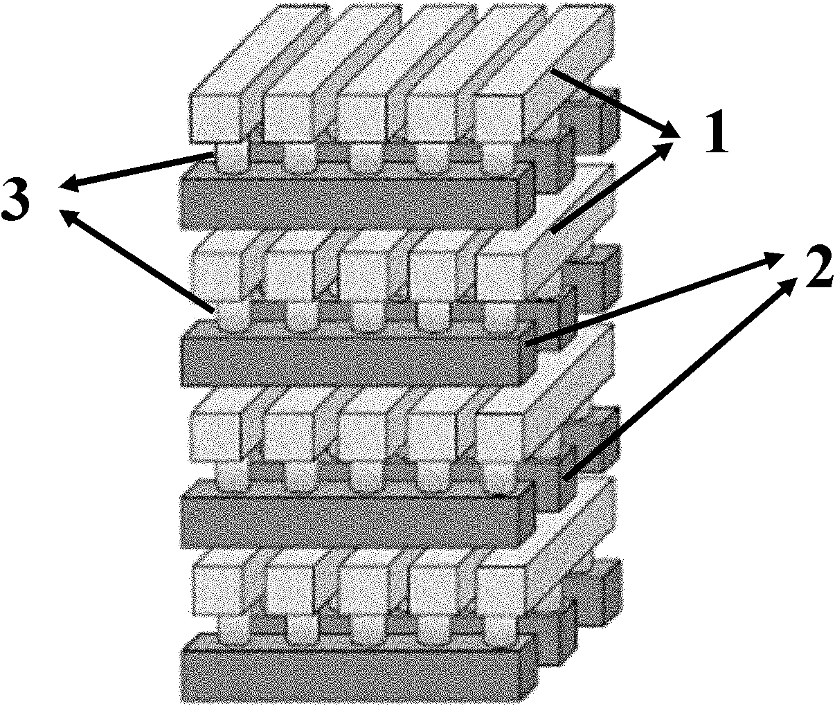
Resistive memory usually adopts a cross bar structure and a multi-layer stacking method to realize a three-dimensional architecture (such as figure 1 ), this method requires photolithography for each layer of electrodes to form a cross-hair structure, so the number of photolithography and etching is proportional to the number of stacked layers, which greatly increases the difficulty and cost of the process

Method used


Image

  • Three-dimensional nonvolatile memory array and preparation method thereof
  • Three-dimensional nonvolatile memory array and preparation method thereof
  • Three-dimensional nonvolatile memory array and preparation method thereof

Examples


Embodiment Construction

[0026] In order to make the above objects, features and advantages of the present invention more comprehensible, specific implementations of the present invention will be described in detail below in conjunction with the accompanying drawings.

[0027] In the following description, a lot of specific details are set forth in order to fully understand the present invention, but the present invention can also be implemented in other ways different from those described here, and those skilled in the art can do it without departing from the meaning of the present invention. By analogy, the present invention is therefore not limited to the specific examples disclosed below.

[0028] Secondly, the present invention is described in detail in combination with schematic diagrams. When describing the embodiments of the present invention in detail, for the convenience of explanation, the cross-sectional view showing the device structure will not be partially enlarged according to the gener...


PUM

PropertyMeasurementUnit
thicknessaaaaaaaaaa
thicknessaaaaaaaaaa
widthaaaaaaaaaa

Abstract

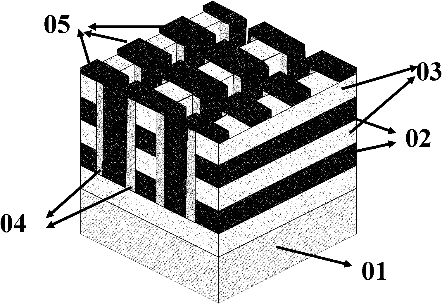
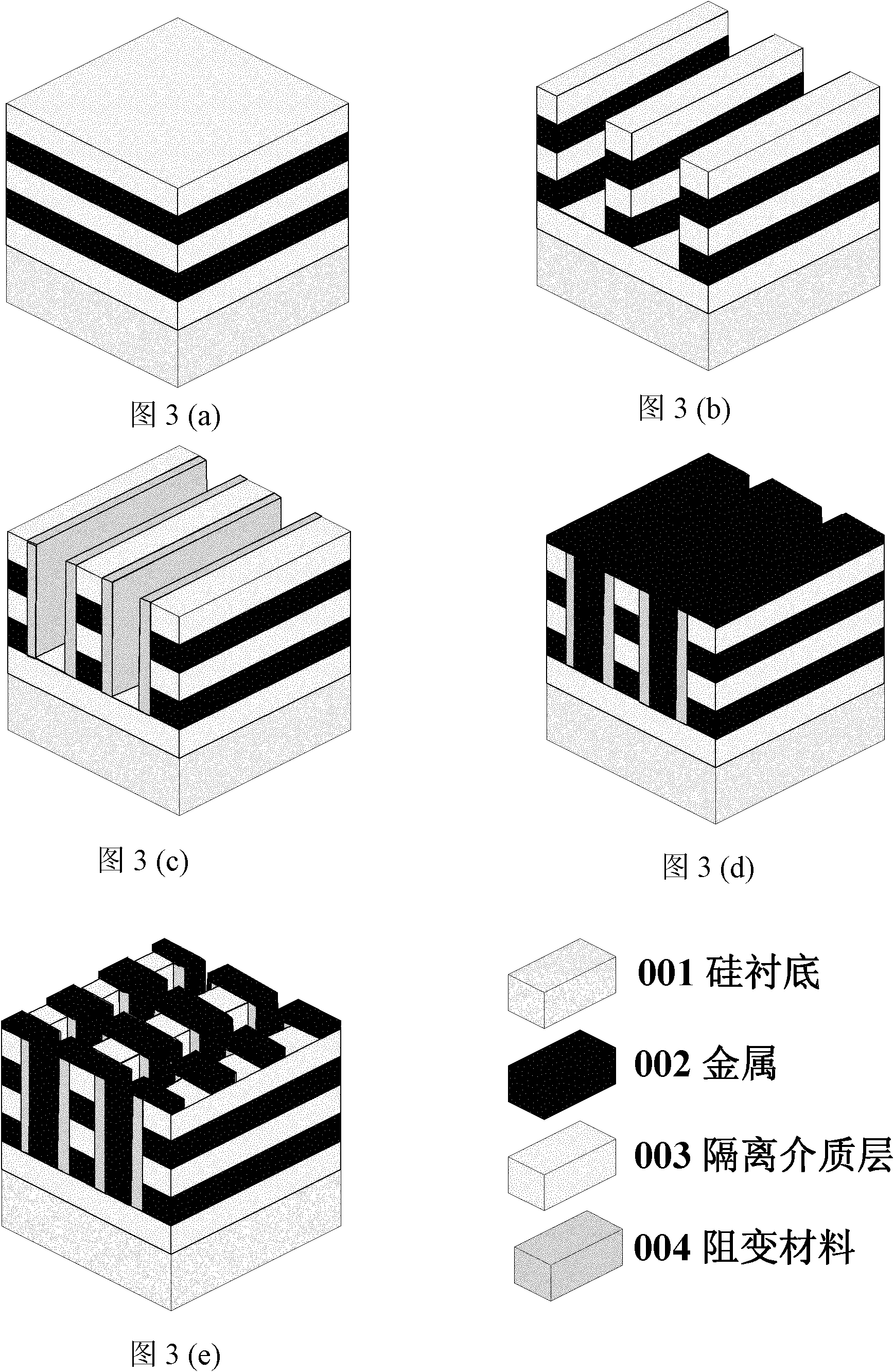
The invention provides a three-dimensional nonvolatile memory array and a preparation method thereof, and belongs to the technical field of a nonvolatile memory in the manufacturing technology of super-large-scale integration. The three-dimensional nonvolatile memory array comprises a substrate and a bottom electrode / isolation medium stack structure; a deep groove is etched on the bottom electrode / isolation medium stack structure; a variable-resistance material and a top electrode layer are deposited on the side wall of the deep groove; the bottom electrode and the top electrode are crossed on the side wall of the deep groove; and a variable-resistance material is arranged between the cross points; each cross point forms a variable-resistance memory unit; all the variable-resistance memory units form a three-dimensional variable-resistance memory array; and the three-dimensional variable-resistance memories in the array are isolated by the isolation medium layer. The invention can improve the storage density of the variable-resistance memory, while simplifying the process and reducing the process cost.

Description

technical field [0001] The invention belongs to the technical field of nonvolatile memory in VLSI manufacturing technology, and in particular relates to a three-dimensional structure nonvolatile memory array and a preparation method thereof. Background technique [0002] Non-volatile memory represented by flash memory is widely used in various products, such as mobile phones, notebooks, handheld computers and solid-state hard disks, because of its data retention ability in case of power failure and its advantages of rewritable data multiple times. communication equipment. Nowadays, flash memory has occupied most of the market share of non-volatile semiconductor memory. However, with the increasing demand for large capacity, low cost, low power consumption and high performance in the information society and the rapid development of semiconductor technology, now Some flash memory technology has been difficult to meet the needs of the development of non-volatile memory technol...

Claims


Application Information

Patent Timeline
Patent Type & Authority Applications(China)
IPC IPC(8): H01L45/00H01L27/24
CPCH01L27/0688H01L27/249H01L45/04H01L45/1691H01L27/101H01L45/146H01L45/1226H10B63/845H10N70/20H10N70/823H10N70/8833H10N70/068
Inventor 蔡一茂黄如秦石强唐粕人张丽杰唐昱
Owner PEKING UNIV
Learn More