Insulated gate bipolar transistor and manufacturing method thereof

A technology of bipolar transistors and insulated gates, applied in the direction of transistors, semiconductor/solid-state device manufacturing, semiconductor devices, etc. The effect of cost reduction

Inactive Publication Date: 2011-02-16
ZHEJIANG UNIV
View PDF4 Cites 28 Cited by
  • Summary
  • Abstract
  • Description
  • Claims
  • Application Information

AI Technical Summary

Problems solved by technology

[0006] The invention provides an insulated gate bipolar transistor, which solves the problem that...

Method used


Image

  • Insulated gate bipolar transistor and manufacturing method thereof
  • Insulated gate bipolar transistor and manufacturing method thereof
  • Insulated gate bipolar transistor and manufacturing method thereof

Examples


Embodiment Construction

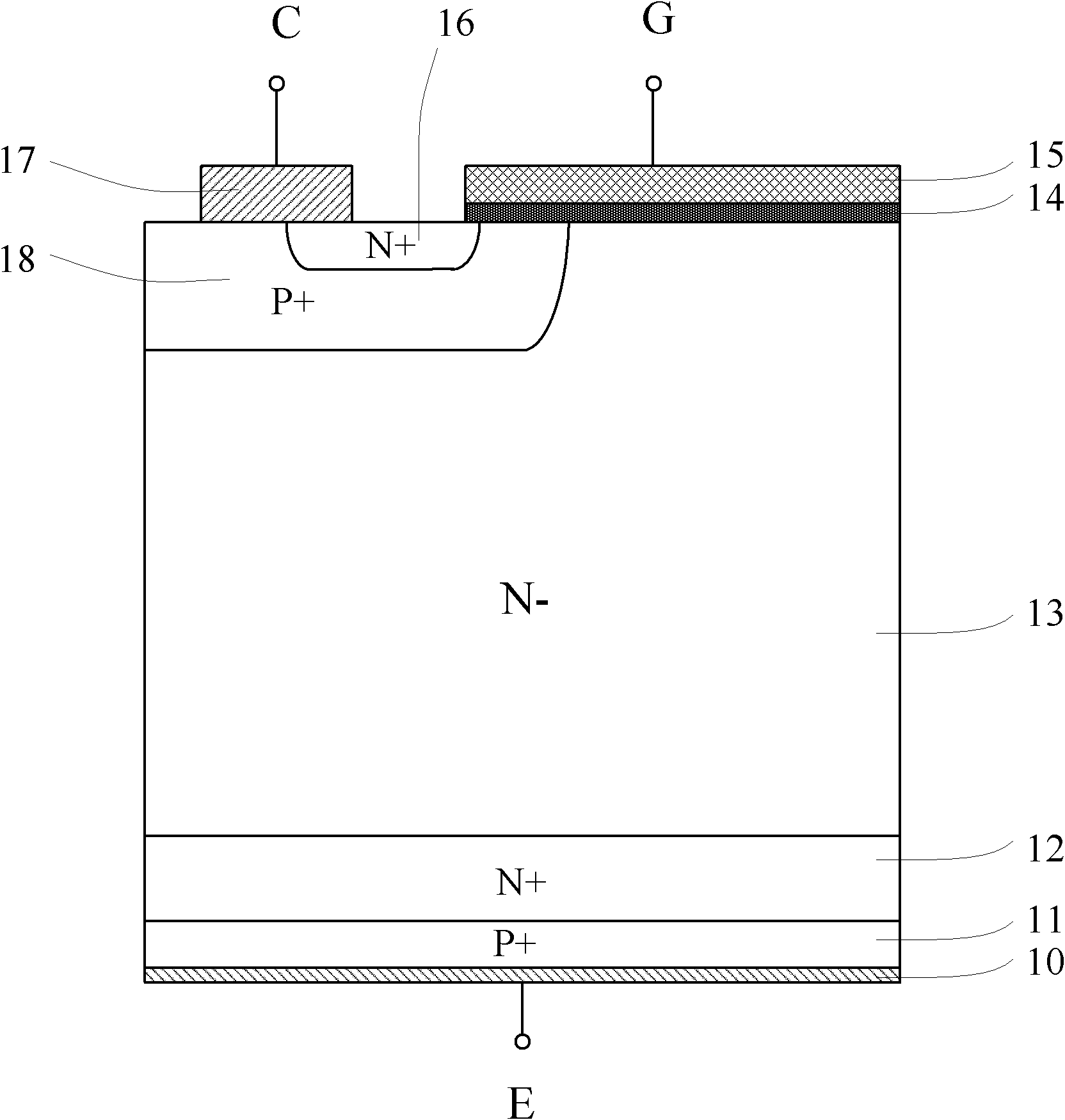
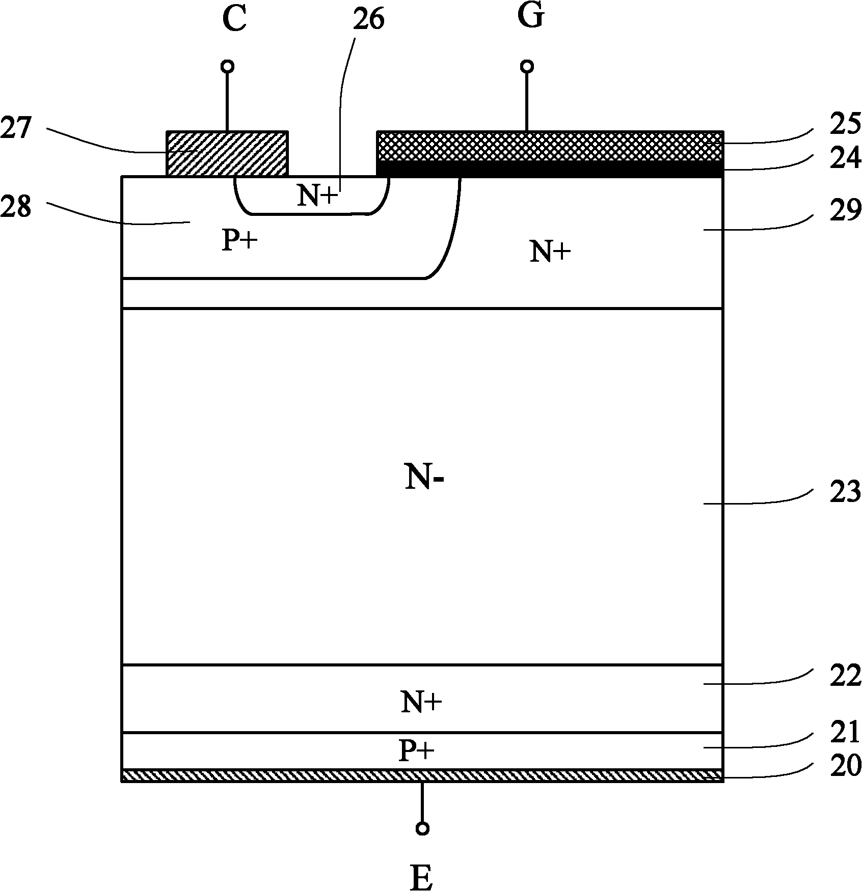
[0022] Such as figure 2 As shown, an insulated gate bipolar transistor includes an N-type base region, a P-type base region 28, a back P+ emitter region 21, an N+ collector region 26, a gate oxide layer 24, a collector electrode 27, a gate electrode 25 and an emitter pole 20, wherein the N base region is composed of an N+ diffused residual layer 29, an N-base region 23 and an N+ buffer layer 22 stacked in sequence. The manufacturing process of the insulated gate bipolar transistor is shown in Figure 3, specifically as follows:

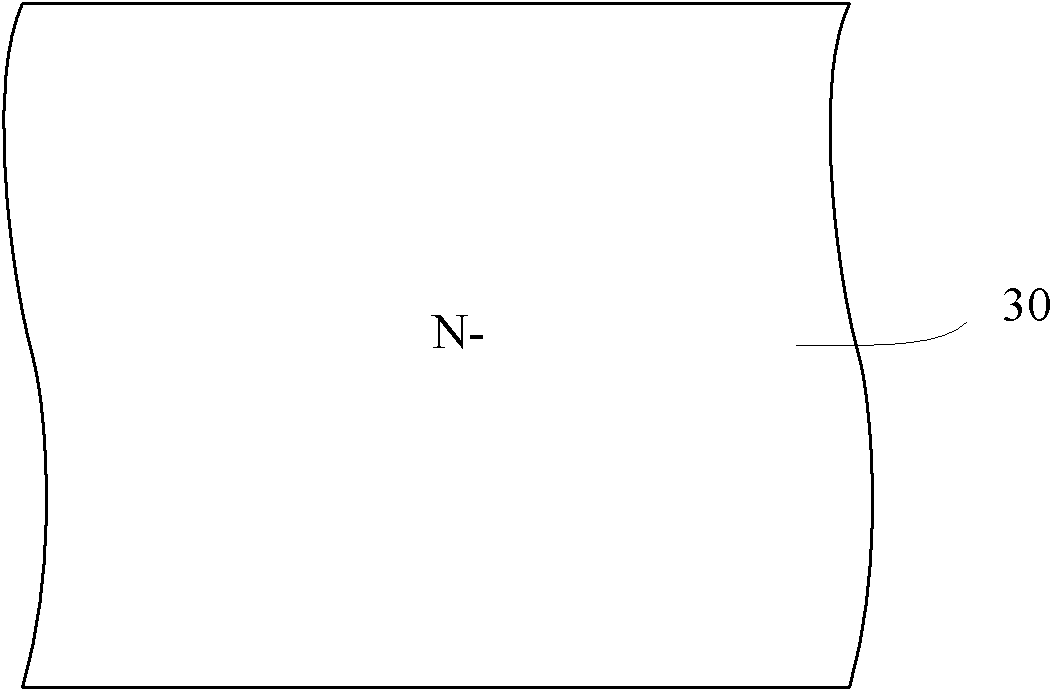
[0023] Such as Figure 3a The N-type single crystal substrate 30 shown has a doping concentration of 6×10 13 cm -3 , the thickness is 500um, and the doping concentration can be adjusted to 4×10 according to the withstand voltage requirement 13 ~1×10 14 cm -3 . Such as Figure 3b As shown, the N-type single crystal substrate is diffused at high temperature to form the first N+ diffusion region 32, the N-base region 23 and the second N+ diffusion...


PUM

PropertyMeasurementUnit
Thicknessaaaaaaaaaa
Thicknessaaaaaaaaaa
Thicknessaaaaaaaaaa

Abstract

The invention discloses an insulated gate bipolar transistor (IGBT) and a manufacturing method thereof. The IGBT comprises an N-type base region, a P-type base region, a back P+ emitter region, an N+ collector region, a gate oxide, a collector electrode, a gate electrode and an emitter electrode; the N-type base region consists of a N+ diffusion residue layer, a N- base region and an N+ buffer layer which are sequentially laminated; and the dosage concentration of the N+ diffusion residue layer and the N+ buffer layer is gradually increased outwards from a boundary with the N- base region. In the IGBT of the invention, a front surface of the N- base region is provided with the N+ diffusion residue layer, so that the ion dosage concentration of a N-type front surface is improved and the influences on a Junction Field Effect Transistor (JEFT) resistor are reduced; therefore, the voltage drop of the IGBT under a conducting condition is effectively reduced.

Description

technical field [0001] The invention relates to the field of semiconductor power devices and manufacturing, in particular to an insulated gate bipolar transistor and a manufacturing method thereof. Background technique [0002] Insulated Gate Bipolar Transistor (Insulated Gate Bipolar Transistor, hereinafter referred to as IGBT) is a combination of gate voltage control characteristics of Metal Oxide Semiconductor Field Effect Transistor (MOSFET) and low on-resistance of Bipolar Junction Transistor (BJT). The semiconductor power device with all characteristics has the characteristics of voltage control, large input impedance, low driving power, small on-resistance, low switching loss and high operating frequency. It is an ideal semiconductor power switching device and has broad development and application prospects. . [0003] Generally speaking, IGBTs can be divided into two types: punch-through type (PT-IGBT) and non-punch-through type (NPT-IGBT). Punch-type insulated gat...

Claims


Application Information

Patent Timeline
IPC IPC(8): H01L29/739H01L29/06H01L21/331
CPCH01L29/7395H01L29/66333H01L29/0847
Inventor 张斌韩雁张世峰胡佳贤朱大中
Owner ZHEJIANG UNIV
Why Eureka
Try Eureka