
PCB (Printed Circuit Board) production line combining manual in process processing and paster processing

A PCB board and production line technology, applied in the field of PCB wrench plug-in processing and patch processing composite production line, can solve the problems of reducing product defect rate and production cost, long veneer operation time, and high product defect rate, reducing work The effect of personnel and product defect rate reduction, equipment management and maintenance is simple

Active Publication Date: 2011-02-16
NANJING PANDA ELECTRONICS MFG
View PDF5 Cites 41 Cited by
  • Summary
  • Abstract
  • Description
  • Claims
  • Application Information

AI Technical Summary

Problems solved by technology

[0003] The purpose of the present invention is to design a method for fixing long-pin components with UV glue during double-sided reflow soldering of PCBs, aiming at the problems of many operators in the existing production process, high product defect rate, long single-board operation time, and high production costs. Realize the technology of reflow soldering, combine SMT operation and manual insertion operation, which is beneficial to reduce the number of operators, reduce the defective rate of products and the synthetic production line for PCB boards

Method used


Image

  • PCB (Printed Circuit Board) production line combining manual in process processing and paster processing
  • PCB (Printed Circuit Board) production line combining manual in process processing and paster processing
  • PCB (Printed Circuit Board) production line combining manual in process processing and paster processing

Examples


Embodiment Construction

[0048] The present invention will be further described below in conjunction with the accompanying drawings and embodiments.

[0049] Such as Figure 1-11 shown.

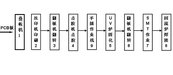
[0050] A composite production line of PCB hand plug-in processing and patch processing, such as figure 1 As shown, it mainly consists of the following equipment:

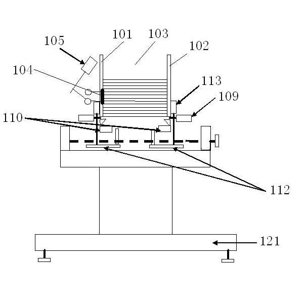
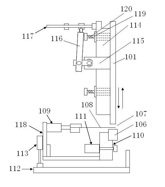
[0051] A board machine 1 (such as figure 2 , 3 shown), the loading machine 1 sends the PCB board placed in the upper board channel into the guide rail of the production line in time according to the production rhythm, and is sent into the adjacent screen printing machine 2 under the drive of the conveyor belt in the guide rail; enter The PCB board in the upper board channel of the board loading machine 1 has undergone SMT patch processing and low temperature reflow processing;

[0052] Screen printing machine 2, the screen printing machine 2 is responsible for silk screen printing of low-temperature solder paste on the PCB board that has been sen...


PUM


Abstract

The invention discloses a PCB (Printed Circuit Board) production line combining a manual in process processing and paster processing, which is characterized by comprising a board feeding machine (1), a screen printing machine (2), as well as a first board overturning machine (3), an adhesive dispenser (4), a UV curing oven (5), a second board overturning machine (6), SMT (Surface Mounting Technology) equipment (7) and a reflow soldering heating curing oven (8). The first board overturning machine (3) is responsible for overturning a PCB subjected to low-temperature solder past printing of the screen printing machine (2) and then dispensing an adhesive, and after adhesive dispensing, a UV adhesive with a large long-pin device is cured under UV irradiation; after the PCB is overturned by the second board overturning machine, the step of paster production begins; and finally, PCB heating curing is finished in the reflow soldering heating curing oven (8). The invention combines SMT operation and manual in process operation together to realize a double-faced reflow soldering technology, solves the defects of traditional wave-soldering technology, and saves energy since reflow soldering is performed only twice and elements are heated twice.

Description

technical field [0001] The invention relates to an electronic printed circuit board production equipment, in particular to a PCB board production line combining hand-inserting and patching, in particular a composite production line of PCB hand-inserting processing and patching processing. Background technique [0002] As we all know, in the production and processing of electronic products, how to reduce the input of personnel, processes and auxiliary materials to achieve the same quality is the key to reducing production costs and improving production efficiency. BPR is such a new production method. In the past production, there are usually two processing methods: the first is two reflow soldering + one wave soldering, which is to first reflow solder the components on both sides of the PCB, and then complete the SMT production line. The PCB board turnover is transferred to the substrate production line for hand-insertion operation and wave soldering; the other is three-time ...

Claims


Application Information

Patent Timeline
IPC IPC(8): H05K3/34H05K13/04H05K3/30
Inventor 于蓉丁卫中王旭辉李海强冯恩忠
Owner NANJING PANDA ELECTRONICS MFG
Learn More