Packaging substrate as well as manufacturing method and base material thereof

A technology for packaging substrates and manufacturing methods, applied in semiconductor/solid-state device manufacturing, electrical components, electrical solid-state devices, etc., can solve the problems of wasting the manufacturing process of the release layer or the adhesive layer, increasing the production cost, and discarding the packaging substrate. The effect of omitting the manufacturing process, saving costs and avoiding waste

Active Publication Date: 2011-03-23
UNIMICRON TECH CORP
View PDF0 Cites 28 Cited by
  • Summary
  • Abstract
  • Description
  • Claims
  • Application Information

AI Technical Summary

Problems solved by technology

[0012] However, the existing manufacturing method needs to additionally form the carrier board 10 and the thin film metal layer 11 to temporarily support the structures on both sides, thus making the manufacturing process more complicated, and eventually the temporary carrier of the middle layer (including the carrier board 10, Two layers of thin film metal layer 11 and two layers of release layer 12), will eventually cause a lot of material waste and increase production costs
[0013] Therefore, in view of the above-mentioned problems, how to avoid the waste and complicated manufacturing process caused by discarding the intermediate temporary carrier and additionally forming a release layer or an adhesive layer on the temporary carrier in the manufacturing method of the prior art packaging substrate, has become an urgent problem to be solved

Method used


Image

  • Packaging substrate as well as manufacturing method and base material thereof
  • Packaging substrate as well as manufacturing method and base material thereof
  • Packaging substrate as well as manufacturing method and base material thereof

Examples


no. 1 example

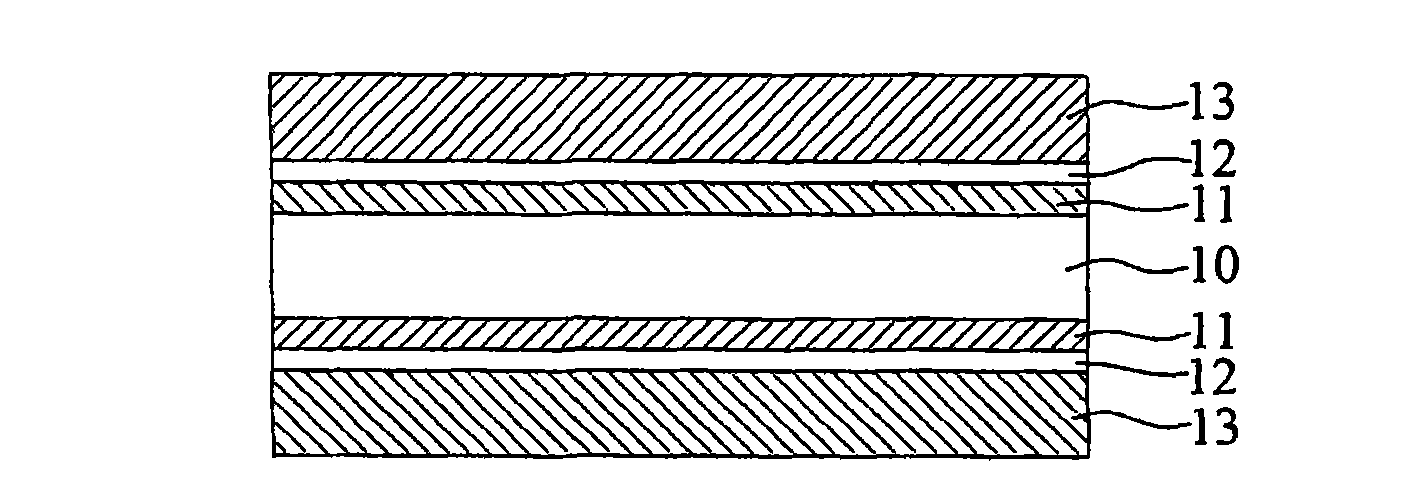
[0094] see Figure 2A to Figure 2F , is a schematic cross-sectional view of the first embodiment of the packaging substrate and its manufacturing method of the present invention.

[0095] Such as Figure 2AAs shown, firstly, two first metal layers 20a, 20b are respectively provided with opposite first surfaces 201a, 201b and second surfaces 202a, 202b and are superimposed with the first surfaces 201a, 201b. The first auxiliary dielectric layer 21a, 21b on the second surface 202a, 202b of the first metal layer 20a, 20b, and the two second metal layers respectively disposed on the exposed surface of the first auxiliary dielectric layer 21a, 21b Layers 22a, 22b, and the second metal layer 22a, 22b may be thicker than the first metal layer 20a, 20b to provide sufficient rigidity.

[0096] In this embodiment, the first surface 201a, 201b may be a smooth surface, and the second surface 202a, 202b may be a rough surface.

[0097] Such as Figure 2B As shown, these first metal lay...

no. 2 example

[0106] see Figure 3A to Figure 3D , is a schematic cross-sectional view of a second embodiment of the packaging substrate and its manufacturing method of the present invention.

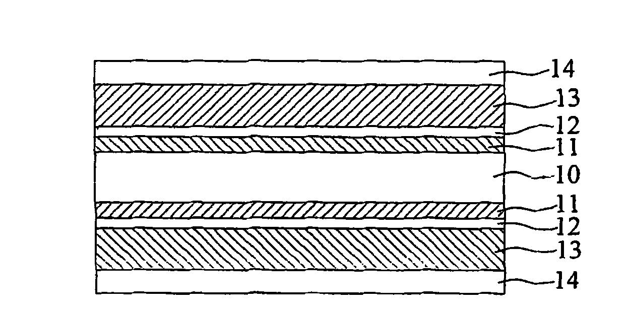
[0107] Such as Figure 3A shown, continued from Figure 2C In the manufacturing method, the first circuit layer 232a, 232b of the outermost layer of the build-up structure 23a, 23b also has a plurality of first electrical contact pads 234a, 234b; and then on the outermost layer of the build-up structure 23a, 23b Form the first insulating protective layers 25a, 25b, such as solder resist layers, and the first insulating protective layers 25a, 25b are respectively formed with a plurality of first insulating protective layers correspondingly exposing each of the first electrical contact pads 234a, 234b. Layer openings 250a, 250b.

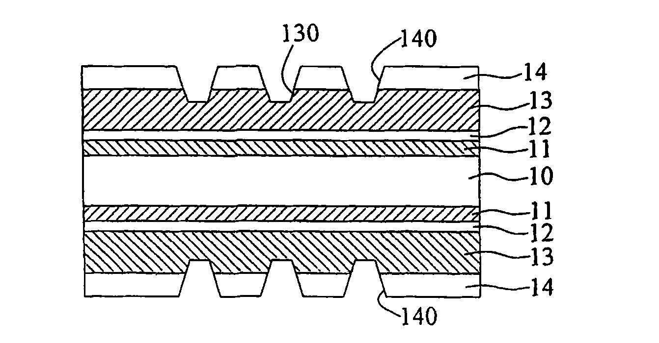
[0108] Such as Figure 3B As shown, the trimming is along the edges of the monolithic structure, and the trimming edge 24 passes through the first metal layer 20a, 20b. ...

no. 3 example

[0112] see Figure 4A to Figure 4F , is a schematic cross-sectional view of the third embodiment of the packaging substrate and its manufacturing method of the present invention, wherein, the Figure 4E' and Figure 4F' It is another implementation form of this embodiment.

[0113] Such as Figure 4A shown, continued from Figure 2B According to the manufacturing method, the second metal layer 22a, 22b is subjected to a patterned manufacturing process to form inner layer circuit layers 301a, 301b, and a plurality of electrical connections to the inner layer circuit layers are formed in the first auxiliary dielectric layer 21a, 21b layers 301a, 301b and the inner layer conductive blind holes 302a, 302b of the first metal layer 20a, 20b, and build-up structures 23a, 23b are formed on the first auxiliary dielectric layer 21a, 21b and the inner layer circuit layer 301a, 301b , the build-up structure 23a, 23b includes at least one first dielectric layer 231a, 231b, a first circ...


PUM

PropertyMeasurementUnit
thicknessaaaaaaaaaa

Abstract

The invention discloses a packaging substrate as well as a manufacturing method and a base material thereof. The manufacturing method of the packaging substrate comprises the following steps: two metal layers are mutually laminated, and a dielectric layer is utilized to clad the two metal layers; next, layer increasing line structures are respectively formed at the two sides of the dielectric layer; and finally, the layer increasing line structures at the two sides of the dielectric layer are separated along the interface of the two metal layers so that two packaging substrates are formed. In the invention, the adhesion characteristics of the dielectric layer is utilized so that the two metal layers in the middle cannot be separated in the course of forming the layer increasing line structures in the initial stage, and the dielectric layer part around the two metal layers is cut off to successfully separate the two metal layers so that the manufacturing process is simplified, and the two metal layers in the middle can form a line layer, a metal lug or a supporting structure through the pattering manufacturing process and have no waste.

Description

technical field [0001] The invention relates to a packaging substrate, its manufacturing method and base material, in particular to a low-cost packaging substrate, its manufacturing method and base material. Background technique [0002] With the vigorous development of the electronic industry, electronic products are gradually developing towards the trend of multi-function and high performance. In order to meet the packaging requirements of high integration and miniaturization of semiconductor packages for more active and passive components and circuit loading, semiconductor packaging substrates have gradually evolved from double-layer circuit boards to multi-layer circuit boards ( multi-layer board), so as to use the interlayer connection technology (interlayer connection) in a limited space to expand the available circuit layout area on the semiconductor package substrate, and can cooperate with the use of high circuit density integrated circuits (integrated circuit) Req...

Claims


Application Information

Patent Timeline
Patent Type & Authority Applications(China)
IPC IPC(8): H01L23/498H01L23/48H01L23/12H01L21/48
CPCH01L2224/16225H01L2224/32225H01L2224/48091H01L2224/48227H01L2224/73204H01L2224/73265H01L2924/15174H01L2924/15311
Inventor 刘谨铭
Owner UNIMICRON TECH CORP
Why Eureka
Try Eureka