Method for constructing floating gate

A floating gate and structure technology, applied in the field of semiconductor integrated circuit manufacturing, can solve problems affecting device performance, silicon substrate damage, transistor leakage, etc., and achieve the effect of reducing production costs and simplifying the process.

Active Publication Date: 2012-09-26
SEMICON MFG INT (SHANGHAI) CORP +1
View PDF0 Cites 0 Cited by
  • Summary
  • Abstract
  • Description
  • Claims
  • Application Information

AI Technical Summary

Problems solved by technology

In this way, in the subsequent polysilicon etching process, the polysilicon layer here is quickly consumed in advance because it is thinner than the normal thickness of the polysilicon layer area, resulting in damage to the underlying silicon substrate after the polysilicon etching of the entire time, resulting in transistor Leakage can affect device performance

Method used


Image

  • Method for constructing floating gate
  • Method for constructing floating gate
  • Method for constructing floating gate

Examples


Embodiment Construction

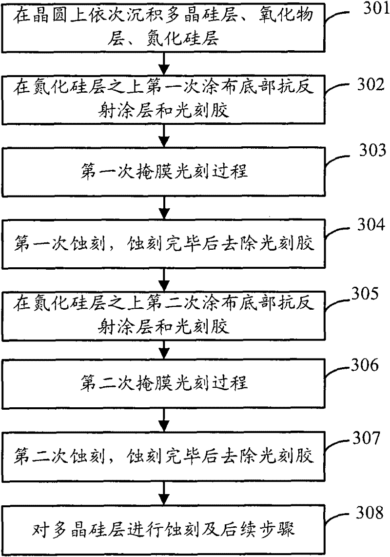
[0028] Aiming at the problems existing in the prior art, the present invention improves the construction process of FG, only coats photoresist and anti-reflection layer once, still adopts two photomasks, exposes twice in succession, and then develops once, but only uses One etching process can avoid the problem that the polysilicon layer is consumed in advance due to excessive consumption of silicon nitride in some areas.

[0029] In order to make the purpose, technical solution and advantages of the present invention clearer, the present invention will be further elaborated below in conjunction with the accompanying drawings.

[0030] The process of constructing the floating gate proposed by the embodiment of the present invention is as follows Figure 4 shown, including the following steps:

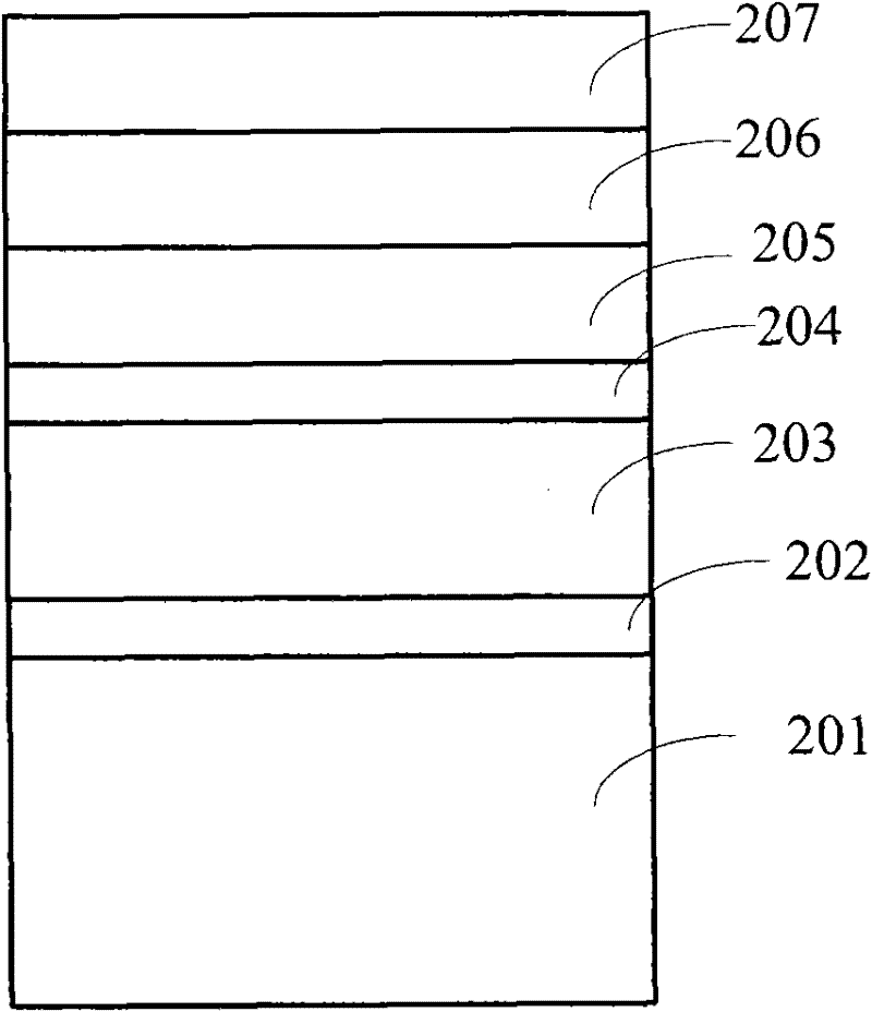
[0031] Step 401: sequentially depositing a gate oxide layer, a polysilicon layer, an oxide layer and a silicon nitride layer on the upper surface of the wafer.

[0032] Step 402: coat...


PUM

PropertyMeasurementUnit
thicknessaaaaaaaaaa
thicknessaaaaaaaaaa

Abstract

The invention discloses a method for constructing a floating gate. The method comprises the following steps: depositing a gate oxygen layer, a polycrystalline silicon layer, an oxide layer and a silicon nitride layer in turn on the upper surface of a wafer; coating photoresist on the silicon nitride layer; performing the first exposure on the photoresist by using a photomask with an x-direction strip pattern; performing the second exposure on the photoresist by using a photomask with a y-direction strip pattern and developing, and defining an x-direction strip pattern and a y-direction strip pattern on the photoresist, wherein the y direction is vertical to the x direction; and etching the silicon nitride layer of the wafer by taking the photoresist as a mask, and then removing the photoresist on the surface of the wafer. In the scheme of the invention, as only once etching is performed on the silicon nitride layer, the thickness unevenness of the polycrystalline silicon layer is avoided. Moreover, due to two photomasks, the outer corner of floating gate(FG) is kept as a right angle, and the performance loss of a grid is prevented.

Description

technical field [0001] The invention relates to the technical field of semiconductor integrated circuit manufacturing, in particular to a construction method of a floating gate (Floating Gate, FG). Background technique [0002] The stacked gate structure (Stack-gate) of the floating gate and the control gate is widely used in the manufacturing process of the memory cell of the split-gate-flash (Split-gate-flash). The outline of the floating gate is of great significance to the electrical performance of the device. [0003] figure 1 is a top view of the flash surface area. Each of the FGs is convex relative to its surrounding area. An important step in the construction of FG is to define the shape of FG, including the process of lithography and etching: [0004] Coating photoresist on the surface of the wafer, exposing the surface of the wafer with a photomask with a pre-defined pattern, transferring the pre-defined pattern on the photomask to the photoresist, and then us...

Claims


Application Information

Patent Timeline
Patent Type & Authority Patents(China)
IPC IPC(8): H01L21/28H01L21/336H01L21/8247
Inventor 王友臻宋建鹏
Owner SEMICON MFG INT (SHANGHAI) CORP
Why Eureka
Try Eureka