

Surface passivation method for Ge
A thin film and solution technology, applied in electrical components, semiconductor/solid-state device manufacturing, circuits, etc., can solve the problems of degraded MOS device performance, high defect density, low dielectric constant, etc.
- Summary
- Abstract
- Description
- Claims
- Application Information
AI Technical Summary
Problems solved by technology
Method used
Image

Examples
Embodiment Construction
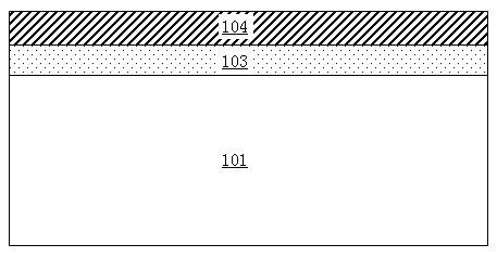
[0016] The present invention will be further described in detail below in conjunction with the accompanying drawings and specific embodiments. In the drawings, for the convenience of illustration, the thicknesses of layers and regions are enlarged or reduced, and the sizes shown do not represent actual sizes. Although these figures do not fully reflect the actual size of the device, they still completely reflect the mutual positions between the regions and the constituent structures, especially the upper-lower and adjacent relationships between the constituent structures.
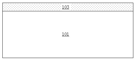
[0017] First, configure CH with a concentration of 1mol / L 3 CSNH 2 solution, and then put the chemically cleaned Ge chip into the configured CH 3 CSNH 2 The Ge wafers were passivated at a temperature of 50 °C for 10 minutes in the solution.
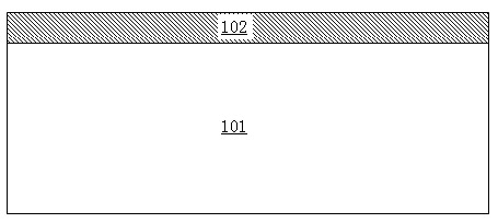
[0018] A thin layer of GeO will adhere to the surface of the Ge sheet 101 after chemical cleaning. x (xfigure 1 shown. After passivation, the GeO attached to the ...
PUM
 Abstract
Description
Claims
Application Information