MOS switching circuit with broadband and high linearity

A switching circuit, high linearity technology, applied in the field of MOS switching circuit, can solve the problems of inability to meet the use of advanced ADC, high switching cost, and time-consuming startup, to eliminate non-ideal factors, good signal linearity, high noise-free The effect of diffuse dynamic range

Inactive Publication Date: 2011-04-20
FUDAN UNIV
View PDF0 Cites 16 Cited by
  • Summary
  • Abstract
  • Description
  • Claims
  • Application Information

AI Technical Summary

Problems solved by technology

[0004] First, the small-sized switch handles a small frequency band, which cannot meet the use of advanced ADCs;
[0005] Second, when the small-sized switch processes high-frequency signals, the impedance changes drastically, resulting in poor linearity and serious distortion of the signal;
[0006] Third, although the large-size switch of the traditional MOS process also has good high-frequency performance, it has large parasitic effects and poor low-frequency accuracy
[0007] In response to the above problems, there are currently sampling switches made using the BiCMOS process, such as Analog Devices' "16-Bit, 80MSPS/105MSPS ADC" (Analog Devices AD9640datasheet), etc., which have better ban...

Method used


Image

  • MOS switching circuit with broadband and high linearity
  • MOS switching circuit with broadband and high linearity
  • MOS switching circuit with broadband and high linearity

Examples


Embodiment Construction

[0016] In order to make the object, technical solution and advantages of the present invention clearer, the present invention will be further described in detail below in conjunction with the accompanying drawings.

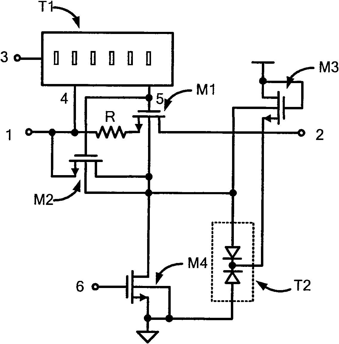
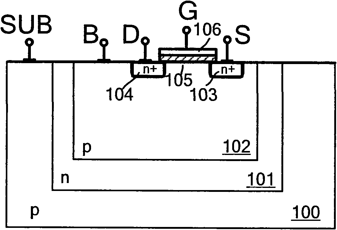
[0017] figure 1 A MOS switch circuit with wideband high linearity is shown as an embodiment of the present invention. like figure 1 As shown, it includes a first input terminal 1 and a first output terminal 2; a gate voltage bootstrap circuit T1 includes a first clock signal 3, a second input terminal 4 and a second output terminal 5; combined as figure 2 As shown in the schematic diagram of the structure of the MOS transistor, it can be seen that the p-type well region 102 forming the MOS transistor is arranged on the n-type deep well region 101, and the n-type deep well region 101 is arranged on the p-type substrate 100 above; the first enhancement MOS transistor M1 is formed in the first p-type well region, its source terminal is connected to the first input...


PUM


Abstract

The present invention belongs to the technical field of integrated circuit, specifically to a MOS switching circuit with broadband and high linearity. A MOS switch is the main body of the circuit; a grid voltage bootstrap circuit is used for stabilizing a switching tube grid source voltage; a substrate bias effect and a switch source drain parasitic junction capacitance are eliminated by isolating a substrate and enabling the substrate to follow an input signal when the switch is conducted; influences of the parasitic junction capacitance between the substrate and an isolated trap by a pre-charge-suspension structure. The main non-ideal factors of non-linearity generated by a common MOS switch are eliminated by the three aspects; and the linearity of the switch under high, middle and low frequency input signals is improved.

Description

technical field [0001] The invention belongs to the field of integrated circuits, and in particular relates to a MOS switch circuit with wide band and high linearity. Background technique [0002] The design of high-speed, high-precision and low-power analog-to-digital converter (ADC) is the development focus of today's mixed-signal system chip design, and it has a wide range of applications in wireless communication, instrument measurement, military radar and high-definition digital TV. . With the development of software-defined radio (SDR) communication technology in the future, it is increasingly required that the digital part of the transceiver system be as close as possible to the antenna end, and the signal processing work after the intermediate frequency is all handed over to digital processing chips that can be flexibly configured. Therefore, the ADC needs to sample in the intermediate frequency band or even the radio frequency band. This requires that the sampling...

Claims


Application Information

Patent Timeline
IPC IPC(8): H03K17/687
Inventor 任俊彦罗磊林楷辉余北朱瑜叶凡许俊李宁李巍
Owner FUDAN UNIV
Why Eureka
Try Eureka