Manufacturing method of active matrix organic light-emitting display array base plate

A light-emitting display and active matrix technology, which is applied in the field of manufacturing the array substrate of the active matrix organic light-emitting display, can solve the problems of reducing production capacity, restricting the development of high-generation LCD or AMOLED production lines, and additional consumption of laser sources, so as to increase production capacity, Satisfy the requirements of carrier mobility and drive TFT's requirements for consistency, and save consumption

Active Publication Date: 2011-04-27
KUNSHAN NEW FLAT PANEL DISPLAY TECH CENT
View PDF2 Cites 18 Cited by
  • Summary
  • Abstract
  • Description
  • Claims
  • Application Information

AI Technical Summary

Problems solved by technology

This not only results in additional consumption of the laser source, but also reduces productivity
At the same time, the crystallization technology of lar

Method used


Image

  • Manufacturing method of active matrix organic light-emitting display array base plate
  • Manufacturing method of active matrix organic light-emitting display array base plate
  • Manufacturing method of active matrix organic light-emitting display array base plate

Examples


Embodiment 1

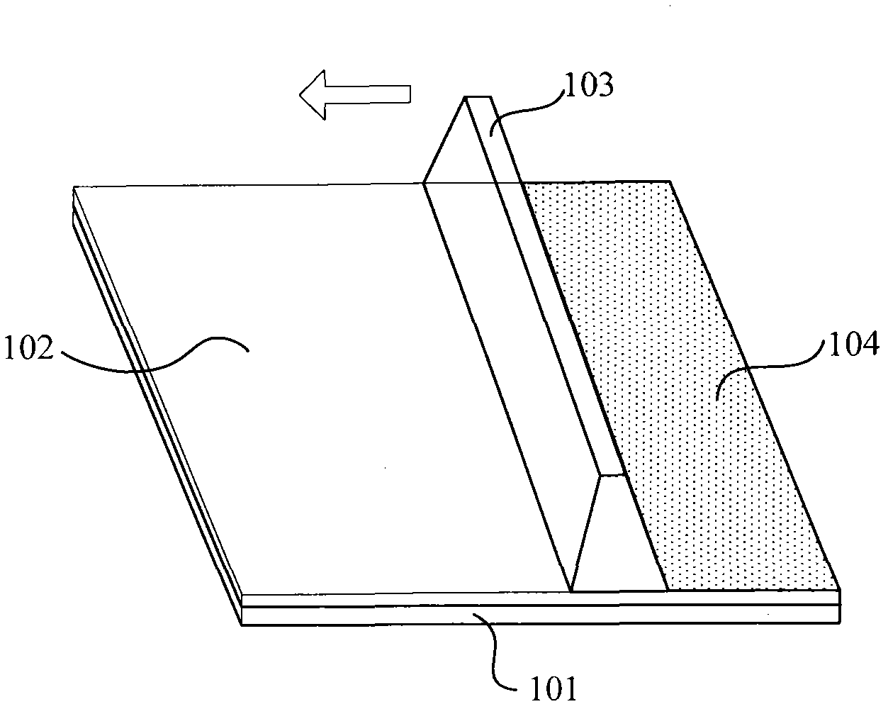
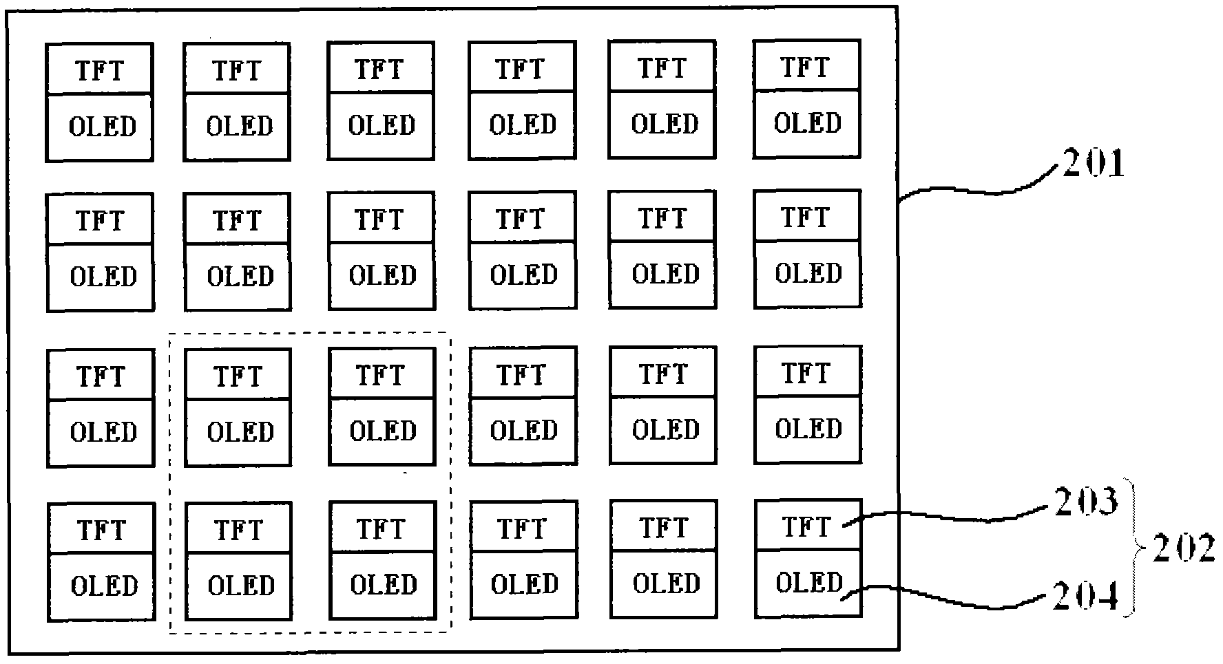
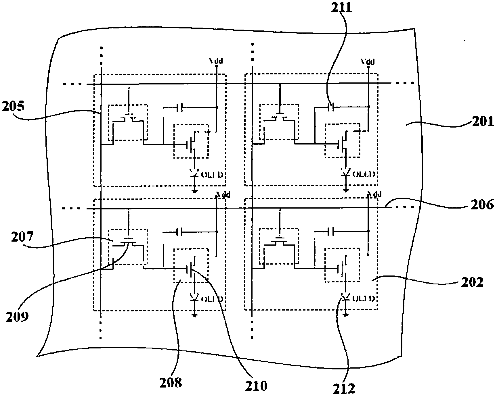
[0031] Figure 2A It is a schematic structural diagram of an active matrix organic light emitting display array substrate, Figure 2B for Figure 2A The enlarged circuit diagram of the dotted line area in the middle, Figure 2C for Figure 2A Schematic diagram of the device structure of a single pixel in . As shown in the figure, the array substrate includes a glass substrate 201, and a plurality of pixels 202 arranged on the substrate are arranged in a matrix. Each pixel 202 includes a TFT region 203 and an OLED region 204, and pixels arranged in parallel between pixels A plurality of data lines 205, and a plurality of scan lines 206 arranged in parallel between the pixels and perpendicular to the data lines. Figure 2B for Figure 2A The enlarged circuit schematic diagram of the dotted line area in the middle, as shown in the figure, the pixel area of ​​the pixel 202 has a switch area 207 and a drive area 208, the switch area 207 has a switch thin film transistor 209, a...


PUM


Abstract

The invention relates to a manufacturing method of an active matrix organic light-emitting display array base plate, in particular to a manufacturing method of a low-temperature polysilicon thin film transistor array base plate. In the technical scheme provided by the invention, solid-phased crystallization is carried out on a noncrystalline silicon layer, and then a switch region is irradiated by a dot matrix laser source so that the carrier mobility for switching on or off a thin film transistor is improved, different requirements of an active matrix organic light-emitting display on the characteristics of driving and switching on or off the thin film transistor are met, meanwhile, the consumption on laser sources is reduced, the production capacity is improved and the method is free from the limit of the size of the array base plate.

Description

technical field [0001] The invention relates to a method for manufacturing an array substrate of an active matrix organic light-emitting display, in particular to a method for manufacturing a low-temperature polysilicon thin film transistor array substrate. Background technique [0002] Low temperature polysilicon thin film transistor (LTPS TFT) array substrates have been widely used in flat panel displays, such as active matrix liquid crystal displays (AMLCDs), active matrix organic light emitting displays (AMOLEDs), and the like. This type of display generally deposits an amorphous silicon layer (a-Si) on the substrate first, and then melts and crystallizes the amorphous silicon through heat treatment to form a smoother polysilicon layer (p-Si) with crystal grains. layer as the channel layer of the thin film transistor (TFT), making the array substrate. [0003] At present, for LTPS crystallization technology, solid phase crystallization (SPC), excimer laser annealing (EL...

Claims


Application Information

Patent Timeline
IPC IPC(8): H01L21/77H01L27/32
Inventor 黄秀颀邱勇魏朝刚陈红
Owner KUNSHAN NEW FLAT PANEL DISPLAY TECH CENT
Why Eureka
Try Eureka