Multilayer stacked storage and manufacture method thereof

A multi-layer stacking and memory technology, which is applied in static memory, read-only memory, semiconductor/solid-state device manufacturing, etc., can solve the problems of unoptimized performance, high cost, and cost reduction, and achieve cost and performance advantages , performance improvement, and the effect of reducing types

Active Publication Date: 2013-03-13
SHANGHAI INST OF MICROSYSTEM & INFORMATION TECH CHINESE ACAD OF SCI
View PDF0 Cites 0 Cited by
  • Summary
  • Abstract
  • Description
  • Claims
  • Application Information

AI Technical Summary

Problems solved by technology

However, the performance of the system using a variety of memory chips still cannot achieve the best state, and the cost is relatively high
At present, there is no unified storage mode that can replace the above-mentioned mixed mode. If there is a high-performance unified mode, the performance of the memory will be further improved, the structure of the electronic system will be further simplified, and the cost will be further reduced.

Method used


Image

  • Multilayer stacked storage and manufacture method thereof
  • Multilayer stacked storage and manufacture method thereof
  • Multilayer stacked storage and manufacture method thereof

Examples


Embodiment 1

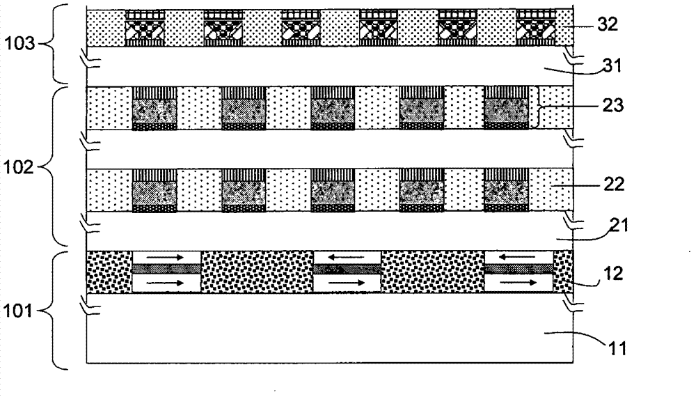
[0042] Figure 1A The schematic diagram of the structure of the resistive switching memory with multi-layer stacking structure is shown, which is better explained, but it does not mean that the present invention is exactly as Figure 1A As shown in this structure, the number of layers, type, size, arrangement and structure of the memory can now be changed, and these are not limiting elements of the present invention.

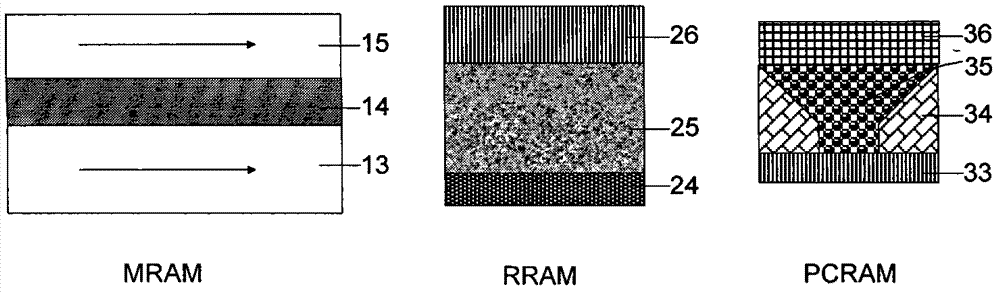
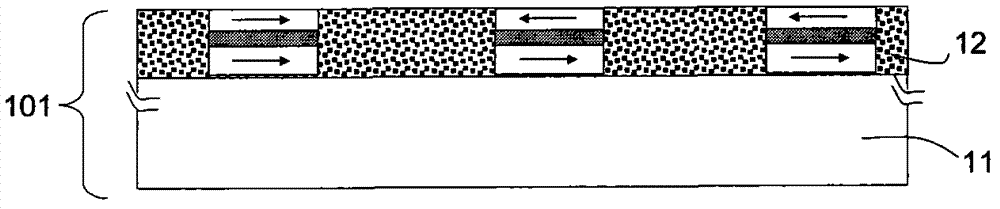
[0043] From Figure 1A It can be seen that the device has a multilayer stack structure, including one MRAM layer 101 , two RRAM layers 102 and one PCRAM layer 103 . Each of the above-mentioned layers not only includes resistive memory cells, but also includes corresponding gate cells (although not shown in the figure, it does not mean that there are none). In addition, layer 101 not only includes magnetoresistive memory units and gating units, but also generally includes peripheral circuits, which are shared by all layers, and play the role of gating and operatin...

Embodiment 2

[0063] In this embodiment, the manufacturing method of the multilayer stacked resistance switching memory of the present invention includes the following steps:

[0064] [Step 1] Manufacture peripheral circuits and two layers of DRAM storage layers on wafer A. These two layers of DRAM cells will be used as high-speed memory.

[0065] [Step 2] Manufacture polysilicon on wafer A using a low-temperature process, manufacture polysilicon diodes and corresponding phase-change memory arrays through semiconductor processes, and obtain polysilicon diode-gated phase-change memory through filling and planarization of dielectric materials layer, the polysilicon diode can be a PN diode or a Schottky diode.

[0066] [Step 3] Continue to deposit polysilicon on the multi-layer memory wafer obtained above to manufacture subsequent storage layers until the desired number of layers is reached.

[0067] 【Step 4】Lead package.

[0068] [Step 5] Practical application. Compared with phase change m...

Embodiment 3

[0070] The invention discloses a method for manufacturing a multi-layer stacked resistance switching memory, comprising the following steps:

[0071] [Step 1] Firstly, the peripheral circuit and the RRAM array are manufactured on the silicon substrate A, wherein the peripheral circuit not only includes the read, write, and erase circuits, but also includes the judgment and sending instruction circuit parts, and the RRAM array is composed of RRAM memory cells and gate transistors. Planarization is achieved after fabrication.

[0072] [Step 2] After doping the silicon substrate B, a PN junction or Schottky barrier is formed, and the PN junction or Schottky barrier will be used to manufacture gate units in subsequent steps.

[0073][Step 3] Transfer the surface layer silicon with a PN junction or Schottky barrier on the surface of the silicon substrate B to the above-mentioned array obtained on the silicon substrate A by bonding, and remove the redundant silicon substrate (can be...


PUM


Abstract

The invention discloses a multilayer stacked storage and a manufacture method thereof. A storage chip comprises a gating unit, a peripheral circuit and at least two storage unit layers, and the storage chip comprises at least two kinds of storage units. During the data storage, the data type requiring processing is judged through the peripheral circuit, and then a command is sent to select the special type of storage to make the best of various storage units and realize the optimization of the storage in various properties. During the actual application, one storage chip can replace a plurality of storage chips so as to achieve the purposes of lowering the cost and improving the property.

Description

technical field [0001] The invention belongs to the technical field of semiconductors, and relates to a memory, in particular to a multi-layer stacked memory; meanwhile, the invention also relates to a method for manufacturing the above-mentioned multi-layer stacked memory. Background technique [0002] Information technology is the pillar industry of today's national economy, semiconductor technology is the cornerstone of information technology, and semiconductor memory is the core component of the semiconductor system. For nearly half a century, the development of semiconductor memory has been changing rapidly, and various types of memory devices have emerged successively. At present, the most widely used storage devices are as follows: dynamic memory (DRAM), static memory (SRAM), magnetic disk, flash memory (FLASH) and so on. These memories have their own characteristics and advantages, and play an irreplaceable role in various fields. In addition, emerging storage tech...

Claims


Application Information

Patent Timeline
Patent Type & Authority Patents(China)
IPC IPC(8): H01L25/065H01L27/115H01L21/98G11C16/02
CPCH01L2924/0002
Inventor 张挺宋志棠刘旭焱刘波封松林
Owner SHANGHAI INST OF MICROSYSTEM & INFORMATION TECH CHINESE ACAD OF SCI
Why Eureka
Try Eureka