Salient point and forming method thereof

A technology of bumps and metal layers under bumps, which is applied in the manufacture of electrical components, electrical solid devices, semiconductor/solid devices, etc., can solve problems such as bridging of bumps, short circuits, and affecting the electrical performance of semiconductor devices, so as to avoid short circuits, The effect of improving electrical performance

Inactive Publication Date: 2011-05-04
SEMICON MFG INT (SHANGHAI) CORP
View PDF1 Cites 1 Cited by
  • Summary
  • Abstract
  • Description
  • Claims
  • Application Information

AI Technical Summary

Problems solved by technology

[0007] As the integration of semiconductor devices becomes higher and higher, the distance between the bumps becomes smaller and smaller. In order to maintain the mechanical strength of the bumps, the height of the bumps must be increased within a limited area; During the pointing process, after the reflow process, due to the physical properties of metal melting, the volume of the bumps will become larger and expand laterally, which may cause bridging between the bumps, which will lead to short circuits and affect the electrical performance of semiconductor devices.

Method used


Image

  • Salient point and forming method thereof
  • Salient point and forming method thereof
  • Salient point and forming method thereof

Examples


Embodiment Construction

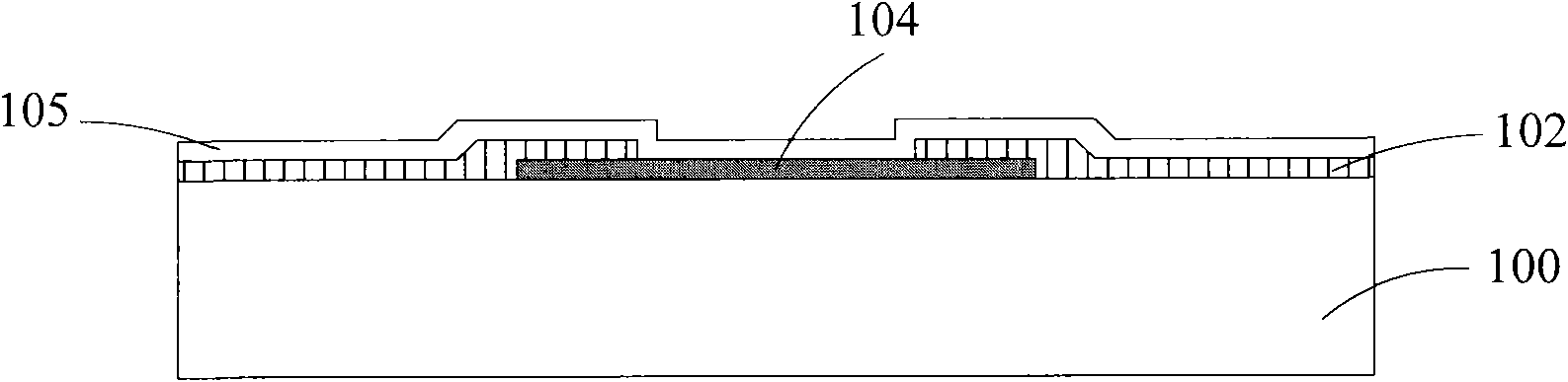
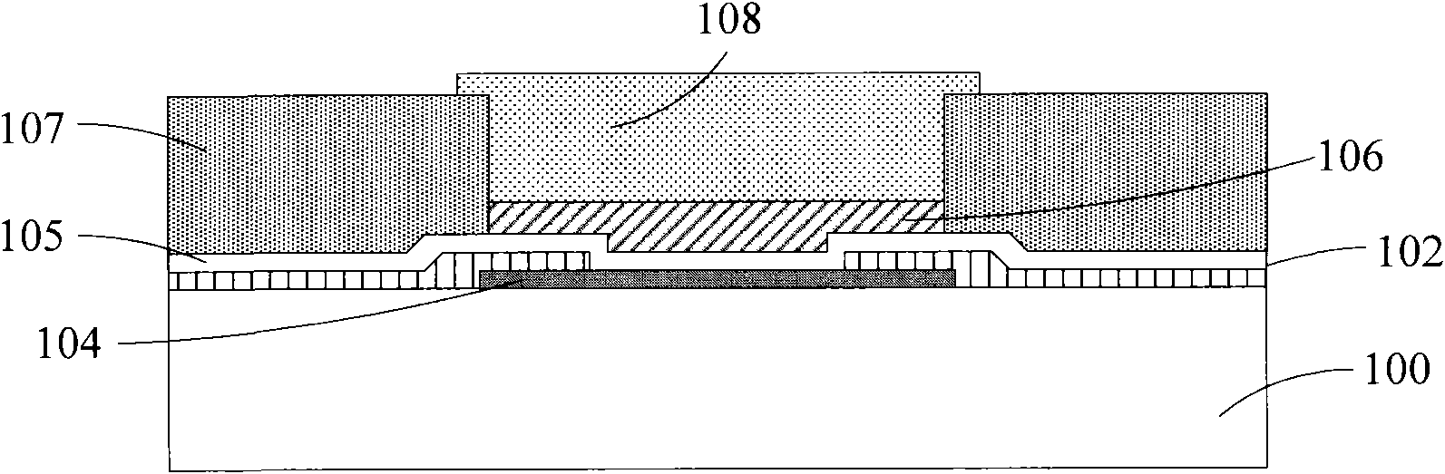
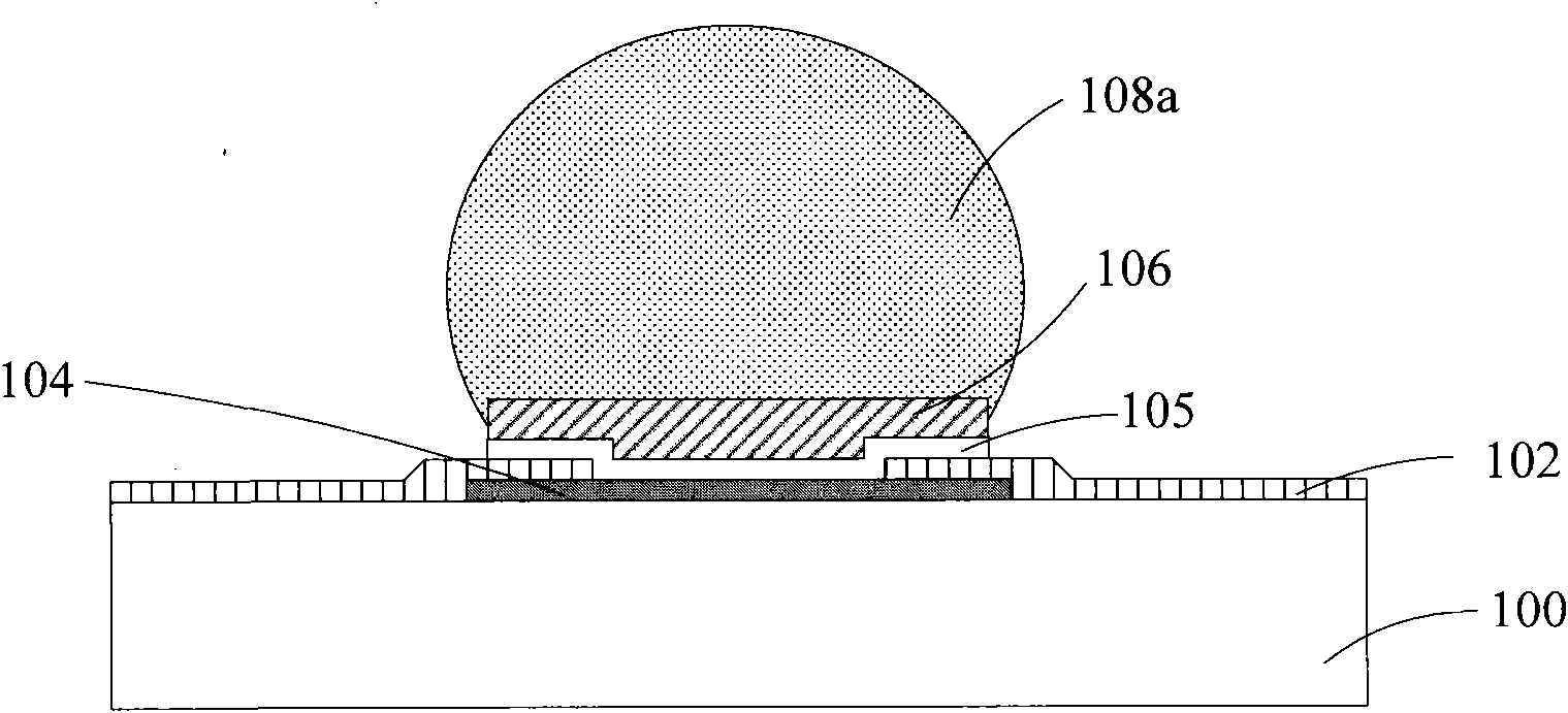
[0027] The present invention provides the concrete flow process of making bump as Figure 4 As shown, step S11 is performed to provide a semiconductor substrate, on which a metal pad layer and a passivation layer are formed, the metal pad layer is embedded in the passivation layer, and exposed through the opening on the passivation layer metal pad layer; perform step S12, form a metal shielding layer on the metal pad layer and the passivation layer in the opening of the passivation layer; perform step S13, form a photoresist layer on the metal shielding layer, on the photoresist layer There is an opening corresponding to the position of the metal pad layer; perform step S14, form a seed layer and an under-bump metal layer on the metal shielding layer in the opening of the photoresist layer; perform step S15, after removing the photoresist layer, etch Removing the metal shielding layer other than the position of the metal pad layer; performing step S16, forming sidewalls on bot...


PUM

PropertyMeasurementUnit
thicknessaaaaaaaaaa
thicknessaaaaaaaaaa
thicknessaaaaaaaaaa

Abstract

The invention relates to a salient point and a forming method thereof, wherein the forming method of the salient point comprises the steps of: providing a semiconductor substrate, wherein a metal cushion layer and a passivation layer are formed on the semiconductor substrate, the metal cushion layer is embedded in the passivation layer and exposes through an opening on the passivation layer; forming metal shielding layers on the metal cushion layer in the opening of the passivation layer and the passivation layer; forming photoetching glue layers on the metal shielding layers, wherein an opening corresponding to the metal cushion layer is arranged on the photoetching glue layer; forming a seed crystal layer and a salient lower metal layer on the metal shielding layer in the opening of the photoetching glue layer; after removing the photoetching glue layer, etching to remove the metal shielding layer outside the metal cushion layer; forming side walls on two sides of the metal shielding layers, the seed crystal layer and the salient lower metal layer; placing the salient point on the salient point lower metal layer; and refluxing the salient point. The invention solves the problem of the bridging among the salient points and avoids the short circuit.

Description

technical field [0001] The invention relates to the field of manufacturing semiconductor devices, in particular to a bump and a method for forming the same. Background technique [0002] With the continuous development of integrated circuit technology, electronic products are increasingly developing in the direction of miniaturization, intelligence, high performance and high reliability. The integrated circuit packaging not only directly affects the performance of integrated circuits, electronic modules and even the whole machine, but also restricts the miniaturization, low cost and reliability of the entire electronic system. With the gradual reduction of the size of the integrated circuit chip and the continuous improvement of the integration level, the electronic industry has put forward higher and higher requirements for the integrated circuit packaging technology. [0003] Flip chip (flip chip) technology is through the solder balls formed on the surface of the chip, s...

Claims


Application Information

Patent Timeline
Patent Type & Authority Applications(China)
IPC IPC(8): H01L21/60H01L23/485
CPCH01L24/11H01L2224/11H01L2924/01322H01L2924/14H01L2924/00H01L2924/00012
Inventor 王津洲
Owner SEMICON MFG INT (SHANGHAI) CORP
Why Eureka
Try Eureka