General packing method for FPGA (field programmable gate array) configurable logical block (CLB)

A programming logic and user-friendly technology, applied in special data processing applications, instruments, electrical digital data processing, etc., can solve problems such as inability to handle functional configurations

Inactive Publication Date: 2011-05-11
FUDAN UNIV
View PDF1 Cites 18 Cited by
  • Summary
  • Abstract
  • Description
  • Claims
  • Application Information

AI Technical Summary

Problems solved by technology

Literature [4] proposed a boxing method FDUMap for Xilinx's early XC3000 and XC4000 series chips,

Method used


Image

  • General packing method for FPGA (field programmable gate array) configurable logical block (CLB)
  • General packing method for FPGA (field programmable gate array) configurable logical block (CLB)
  • General packing method for FPGA (field programmable gate array) configurable logical block (CLB)

Examples


Embodiment Construction

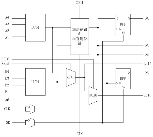
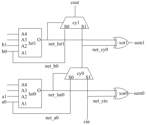
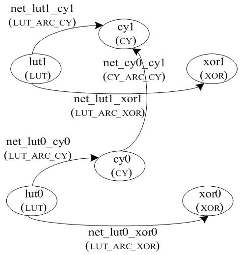
[0080] Assuming that the subscriber circuit adopts figure 2 A two-bit adder in the target graph G u that is image 3 . Figure 7 is the carry chain function circuit of the configurable logic block, and the modeled sample diagram G p Such as Figure 8 shown. The process of solving the two-bit adder bin packing problem with the method of constrained satisfiability problem is as follows:

[0081] (1) The sample graph G p Both vertices and directed edges in are mapped to variable sets X:

[0082] , x LUT Refers to the variable corresponding to the component LUT, x LUT_ARC_XOR Refers to the variable corresponding to the line network LUT_ARC_XOR, and other variables are named in a similar way.

[0083] (2) Put the target graph G u All vertices and directed edges in are mapped to the range D:

[0084] d lut0 Refers to the value corresponding to the element lut0, d net_lut0_xor0 Refers to the value corresponding to net_lut0_xor0, and other values ​​are named in a s...


PUM


Abstract

The invention belongs to the technical field of electronics, in particular to a general packing method for an FPGA (field programmable gate array) configurable logical block (CLB). The method comprises the following steps: configuring and describing chips of the FPGA CLB as a series of directed simple graphs for constraining a satisfaction problem picture matching method; and then identifying a logical function sub-circuit supported by the chip from a user circuit by using the constraint satisfaction problem picture matching method, and packing. According to the invention, only if a library file which describes a target FPGA logical function circuit is pre-defined, the FPGA chips of different structures, such as various functional configurations of a quick carry chain, a distribution type memory, a shift register, an LUT5 (local user terminal 5), an LUT6 (local user terminal 6) and the like can be packed, thereby effectively improving the utilization rate of the logical resources of the chips, and improving the time sequence performance of the circuit. According to the invention, the circuit is optimized according to the appointed requirements, and the mapping of various modularized circuits is realized, thus the method has significant application in system architecture designs and reconfigurable systems.

Description

technical field [0001] The invention belongs to the electronic design automation (Electronic Design Automation, EDA) technical field, and specifically relates to a general packing method for programmable logic blocks in a Field Programmable Gate Array (FPGA, Field Programmable Gate Array). Background technique [0002] The chip structure of field programmable gate array includes programmable logic block (Configurable Logic Block, CLB), programmable input and output (Input Output Block, IOB) and programmable interconnection, with circuit function reconfigurable, short development cycle, design Low cost and other advantages, so it has a wide range of applications in the fields of national defense weapons and equipment, civil communications, automotive electronics and medical treatment. The FPGA software design process mainly includes: logic synthesis, process mapping, packing, placement and routing. Among them, packing is to divide the logic circuit after process mapping acco...

Claims


Application Information

Patent Timeline
IPC IPC(8): G06F17/50
Inventor 王伶俐周学功龚爱慧陈志辉梁绍池
Owner FUDAN UNIV
Why Eureka
Try Eureka