Method for forming semiconductor structure

A semiconductor and graphics technology, applied in semiconductor/solid-state device manufacturing, electrical components, circuits, etc., can solve problems such as large leakage current, high power consumption, and large leakage, so as to save manufacturing costs, do not change the chip area, and save costs Effect

Inactive Publication Date: 2011-05-11
CSMC TECH FAB1 +1
View PDF0 Cites 0 Cited by
  • Summary
  • Abstract
  • Description
  • Claims
  • Application Information

AI Technical Summary

Problems solved by technology

[0003] BiCMOS usually includes a lateral PNP structure. The leakage current of the lateral PNP structure in the existing BiCMOS is relatively large, especially at the process node of 0.5um. The static leakage current of the BiCMOS circuit is large, and the power consumption is high. In severe cases, the entire BiCMOS circuit may even fail to work normally.

Method used


Image

  • Method for forming semiconductor structure
  • Method for forming semiconductor structure
  • Method for forming semiconductor structure

Examples


Embodiment Construction

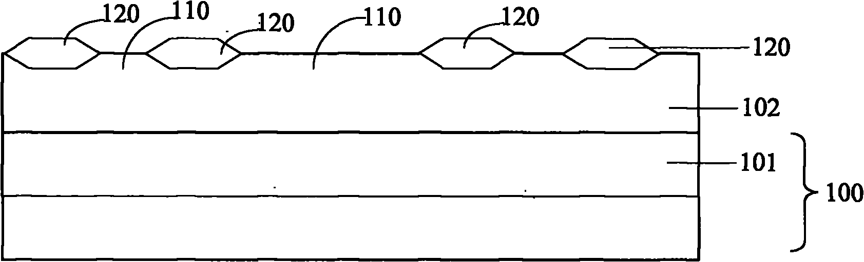
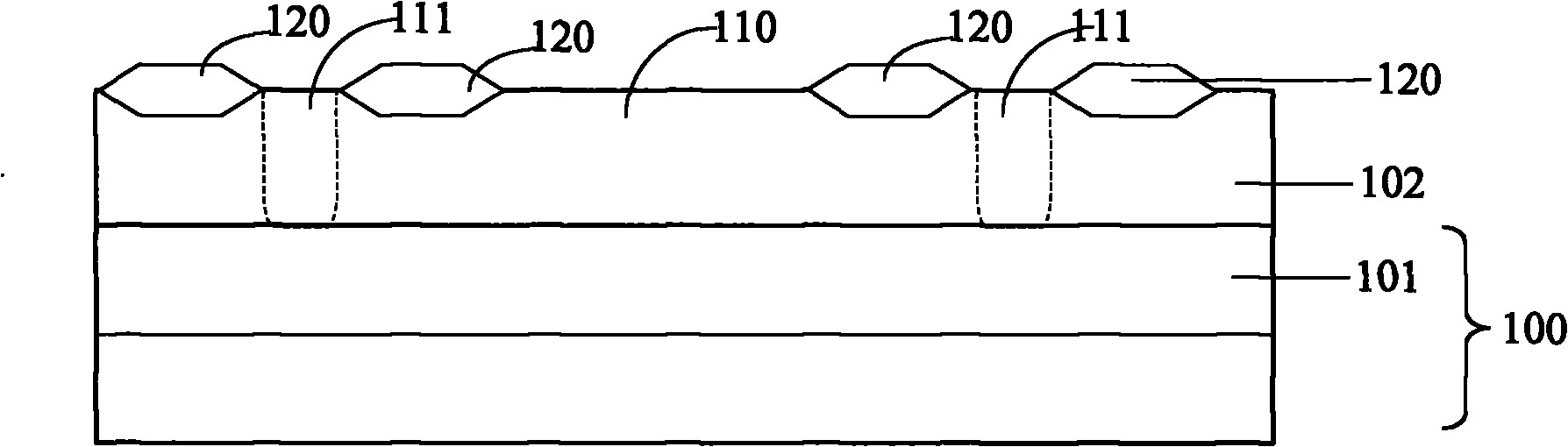
[0016] It can be seen from the background technology that the leakage current of the lateral PNP structure in the existing BiCMOS is relatively large, especially at the process node of 0.5um, the leakage current of the existing PNP structure can reach dozens of nanoamps when the applied voltage is 5V, resulting in the static state of the entire BiCMOS circuit. The leakage current is large, the power consumption is high, and even the entire BiCMOS circuit cannot work normally in severe cases. Usually, the resistivity of the epitaxial layer is adjusted in the process of forming BiCMOS, specifically by adjusting the doping that is generally implanted on the epitaxial layer. Concentration to improve the phenomenon of relatively large leakage in the lateral PNP structure. Another improvement method is to adjust the concentration of the base region of the lateral PNP structure by adding a photolithography process and an implantation process. In addition, the existing process will also...


PUM


Abstract

The invention relates to a method for forming semiconductor structure. The method comprises the following steps: providing a substrate, injecting ions into the substrate so as to form an n buried layer area, forming an n type epitaxial layer on the n buried layer area; forming a plurality of active areas and isolation areas in the n type epitaxial layer, forming an NSINK area on the active area in the n type epitaxial layer, communicating the NSINK area with the n buried layer area; forming a thickened gate-oxide layer on the surface of the epitaxial layer; injecting ions into the surface of the epitaxial layer covered by the gate-oxide layer; forming a gate polycrystalline layer covered by the gate-oxide layer on the surface of the epitaxial layer; injecting ions into the gate polycrystalline layer, forming a side wall on the side walls of the gate-oxide layer and the gate polycrystalline layer, forming an N well in the NSINK area, and injecting ions into the active area so as to form a P well. The invention can reduce the static leaked current of BiCMOS (Bipolar complementary metal oxide semiconductor) circuit.

Description

technical field [0001] The invention relates to the field of semiconductor manufacturing, in particular to a method for forming a semiconductor structure. Background technique [0002] BiCMOS (Bipolar CMOS) is an integrated circuit composed of a bipolar gate circuit and a complementary metal-oxide semiconductor (CMOS) gate circuit. The feature is that the bipolar (Bipolar) process is compatible with the CMOS process, and the bipolar circuit and the CMOS circuit are integrated in a certain circuit form on the same chip, and it has the characteristics of high density, low power consumption, and high-speed and large driving capability. . BiCMOS was proposed and implemented in the early 1980s. It is mainly used in high-speed static memory, high-speed gate array and other high-speed digital circuits. It can also produce excellent analog / digital hybrid circuits for system integration. [0003] BiCMOS usually includes a lateral PNP structure. The leakage current of the lateral PN...

Claims


Application Information

Patent Timeline
Patent Type & Authority Applications(China)
IPC IPC(8): H01L21/8249H01L21/265H01L21/283
Inventor 青云
Owner CSMC TECH FAB1
Why Eureka
Try Eureka