Antimonide transistor with high electron mobility and manufacturing method thereof

A technology with high electron mobility and manufacturing methods, which is applied in semiconductor/solid-state device manufacturing, circuits, electrical components, etc., can solve the problems of no substrate, large lattice mismatch, etc.

Inactive Publication Date: 2011-05-11
INST OF SEMICONDUCTORS - CHINESE ACAD OF SCI
View PDF0 Cites 21 Cited by
  • Summary
  • Abstract
  • Description
  • Claims
  • Application Information

AI Technical Summary

Problems solved by technology

[0004] For antimonide high electron mobility transistors, one of the main problems is that there is no suitable lattice-matched substrate (lattice constant of ), the lattice constant of antimonides is generally in At present, the commonly used semi-insulating GaAs, InP or Si substrates have a large degree of lattice mismatch with them, so how to reduce the large mismatched antimonide high electron mobility transistor structure on these substrates? Defects, improving the quality of epitaxial materials is the key to improving device performance

Method used


Image

  • Antimonide transistor with high electron mobility and manufacturing method thereof
  • Antimonide transistor with high electron mobility and manufacturing method thereof
  • Antimonide transistor with high electron mobility and manufacturing method thereof

Examples


Embodiment Construction

[0098] In order to make the object, technical solution and advantages of the present invention clearer, the present invention will be described in further detail below in conjunction with specific embodiments and with reference to the accompanying drawings.

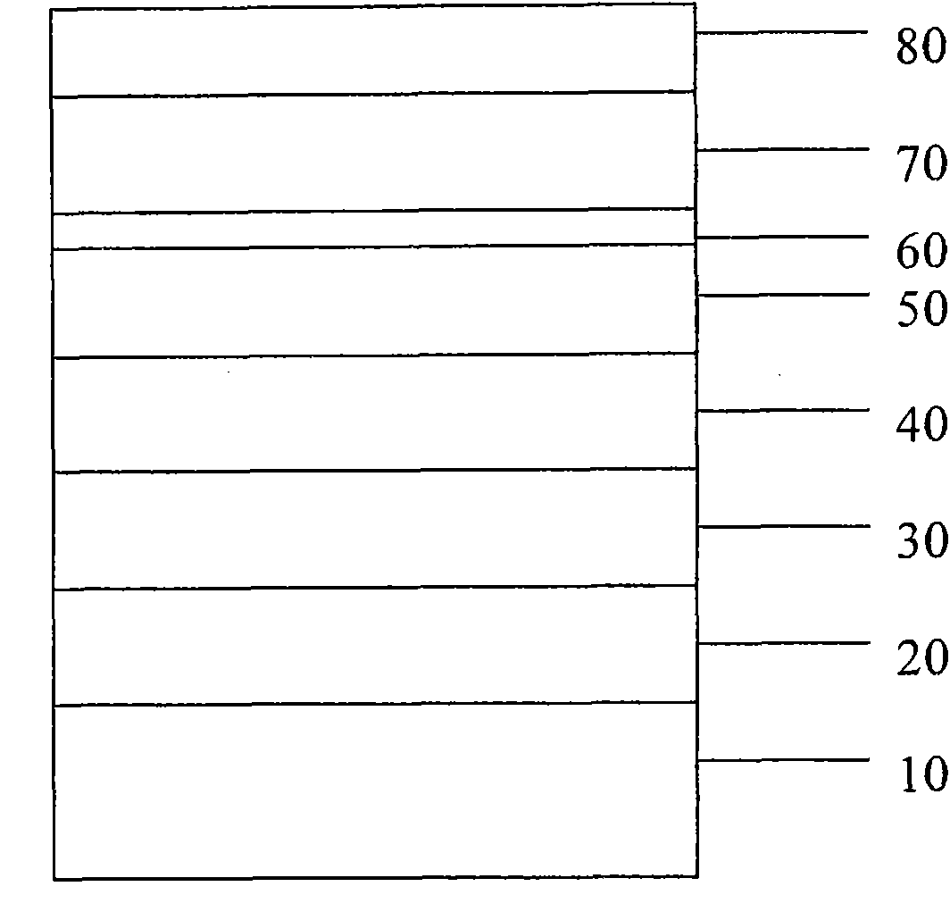
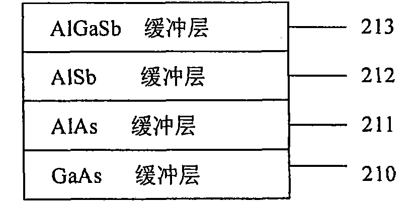
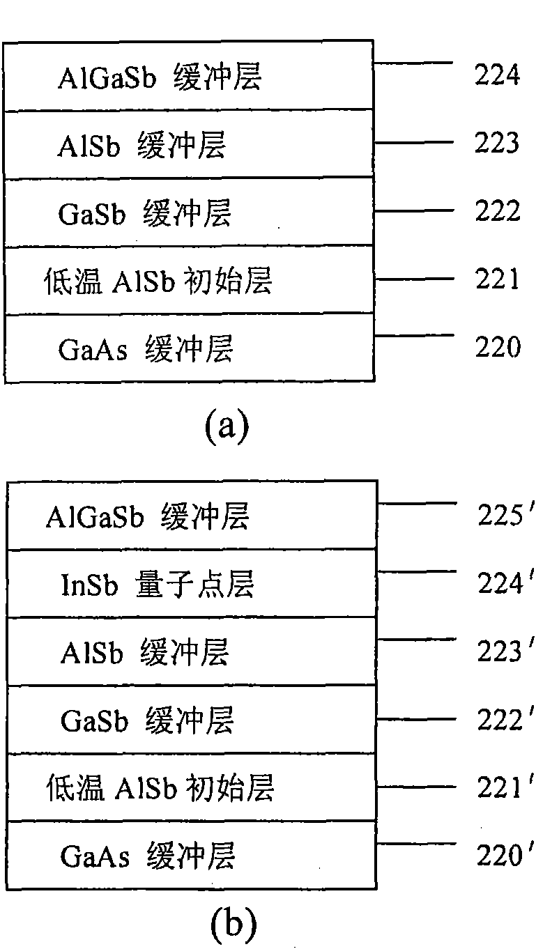
[0099] Such as figure 1 As shown, it is a schematic diagram of the antimonide high electron mobility transistor structure of the present invention, and the antimonide high electron mobility transistor structure includes: a substrate 10, a composite buffer layer 20 grown on the substrate 10, and a composite buffer layer 20 grown on the composite buffer layer 20. The lower antimonide barrier layer 30 on the upper antimonide barrier layer 30, the channel layer 40 grown on the lower antimonide barrier layer 30, the antimonide spacer layer 50 grown on the channel layer 40, the doped antimonide spacer layer grown on the antimonide spacer layer 50 The impurity layer 60 , the upper barrier layer 70 grown on the doped layer 60 , a...


PUM


Abstract

The invention discloses an antimonide transistor with high electron mobility, which comprises a substrate, a composite buffer layer, an antimonide lower barrier layer, a channel layer, an antimonide isolated layer, a doping layer, an upper barrier layer and a cap layer, wherein the composite buffer layer grows on the substrate; the antimonide lower barrier layer grows on the composite buffer layer; the channel layer grows on the antimonide lower barrier layer; the antimonide isolated layer grows on the channel layer; the doping layer grows on the antimonide isolated layer; the upper barrier layer grows on the doping layer; and the cap layer grows on the upper barrier layer. The invention discloses a method for manufacturing the antimonide transistor with the high electron mobility. In the antimonide transistor, by adopting the composite buffer layer, the quality of transistor structural materials is improved greatly, the electronic transport characteristic of a channel is better, the output characteristic of the device is improved, the characteristics of high frequency, high speed and low power consumption of the device is fully played, and the stability and reliability of the device are improved effectively.

Description

technical field [0001] The invention relates to the technical field of semiconductors, in particular to an antimonide high electron mobility transistor and a manufacturing method thereof. Background technique [0002] In high-speed compound semiconductor devices, high electron mobility transistors (HEMT) play a pivotal role. High electron mobility transistors based on III-V compound semiconductors are used in microwave, millimeter wave devices, monolithic integrated circuits and logic integrated circuits. The application of it has received continuous attention in recent years. [0003] The first high electron mobility transistor fabricated was GaAs as the channel layer and AlGaAs as the barrier layer. In order to obtain higher electron mobility and electron velocity (corresponding to higher operating frequency and operating speed), the channel material is changed from GaAs to InGaAs. Typical structure starts with In 0.2 Ga 0.8 As is used as the channel layer, due to the ...

Claims


Application Information

Patent Timeline
Patent Type & Authority Applications(China)
IPC IPC(8): H01L29/778H01L29/06H01L21/335H01L21/20
Inventor 李彦波张杨曾一平
Owner INST OF SEMICONDUCTORS - CHINESE ACAD OF SCI
Why Eureka
Try Eureka