
Diamond wire cutting apparatus and process of silicon wafer for solar cell

A technology of solar cells and cutting equipment, applied in stone processing equipment, fine working devices, manufacturing tools, etc., can solve problems such as environmental pollution, low processing efficiency, large surface damage layer of silicon wafers, etc., to eliminate environmental pollution and improve The effect of processing quality and large output advantages

Inactive Publication Date: 2011-05-18
TIANJIN HUANOU SEMICON MATERIAL TECH CO LTD
View PDF7 Cites 8 Cited by
  • Summary
  • Abstract
  • Description
  • Claims
  • Application Information

AI Technical Summary

Problems solved by technology

Compared with the previous internal circle cutting process, this cutting method using free abrasives has the advantages of cutting large-diameter silicon rods and multiple groups of simultaneous cutting and reducing silicon material consumption, but it also has the following obvious shortcomings: 1. After processing The silicon wafers are polluted by the fat-based abrasive liquid, which increases the difficulty of cleaning the subsequent silicon wafers, resulting in an increase in cleaning costs. 2. The cutting abrasive liquid after use needs to be treated before it can be discharged, which can easily cause environmental pollution; 3. The cutting process is free The material removal mechanism of abrasive particles, which has low processing efficiency due to limited cutting capacity
At present, the main shortcomings of this method are mainly reflected in the following two aspects: 1. Due to the large vibration of the steel wire during the cutting process of the diamond wire saw, the processed silicon wafer produces a large surface damage layer and a large TTV ( total thickness tolerance), which affects the processing quality of silicon wafers
2. The large cutting speed and strong cutting ability of the diamond wire saw will cause a large number of chipping defects in the processed silicon wafers, which will greatly reduce the integrity rate of the silicon wafers, thus affecting its application in the silicon wafer cutting industry

Method used


Image

  • Diamond wire cutting apparatus and process of silicon wafer for solar cell
  • Diamond wire cutting apparatus and process of silicon wafer for solar cell
  • Diamond wire cutting apparatus and process of silicon wafer for solar cell

Examples


Embodiment Construction

[0020] In order to understand the present invention more clearly, describe the present invention in detail in conjunction with accompanying drawing and embodiment:

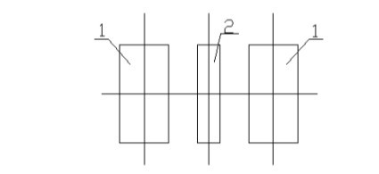
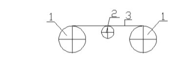
[0021] Such as Figure 1 to Figure 3 As shown in the diamond wire cutting equipment for silicon wafers for solar cells, the guide wheel part includes two main sheaves 1, and a small sheave 2 with a diameter smaller than the main sheave 1 is added between the two main sheaves 1, so that the small sheaves The outer diameter tangent of the upper end of the groove of the sheave 2 coincides with the outer diameter tangent of the upper end of the groove of the two main cutting sheaves 1, and they are installed at the same horizontal position. The shape is the same, the distance from the vertical line of the center of the small sheave 2 to the center of the two main sheaves is equal, and the small sheave 2 is used as a guide wheel for guiding the diamond steel wire passing through the two main cutting sheaves 1, ther...


PUM

PropertyMeasurementUnit
Widthaaaaaaaaaa
Thicknessaaaaaaaaaa

Abstract

The invention relates to a diamond wire saw cutting apparatus and process of a silicon wafer for a solar cell. The diamond wire saw cutting apparatus comprises a guide wheel positioned between two main groove wheels; and through the guiding and transition of the guide wheel, the shake of the diamond steel wire is reduced in the cutting process. The process comprises the following steps: the tension of the diamond wire saw of a silicon bar in the cutting process is 26-28 N; and at the cutting end of the silicon bar, namely, in the cutting process of the remaining 1 / 8-1 / 10, a cutting speed of 0.5-0.7 mm / min is adopted. Through the scheme in the invention, the silicon wafer product yield is greatly increased, the silicon wafer processing quality is relatively good, the problem of environmental pollution caused by the traditional cutting manner of 'naked steel wire plus abrasive slurry' is eliminated, and the scheme has values in application and popularization.

Description

technical field [0001] The invention relates to the field of crystalline silicon chip processing, in particular to a diamond wire cutting device and a process for processing silicon chips for solar cells. Background technique [0002] In recent years, the rapid development of the photovoltaic industry based on solar cell power generation has led to an increasing number of equipment manufacturers related to monocrystalline silicon wafers, and various new types of equipment have emerged in an endless stream, correspondingly producing a variety of silicon wafer processing methods. At present, the mainstream cutting process adopted by most silicon rod cutting processes on the market is "bare steel wire + abrasive slurry". Compared with the previous internal circle cutting process, this cutting method using free abrasives has the advantages of cutting large-diameter silicon rods and multiple groups of simultaneous cutting and reducing silicon material consumption, but it also has...

Claims


Application Information

Patent Timeline
IPC IPC(8): B28D5/04
Inventor 郭红慧刘涛汪雨田王聚安范猛孙红永危晨张雪囡靳立辉王岩沈浩平
Owner TIANJIN HUANOU SEMICON MATERIAL TECH CO LTD
Features
  • Generate Ideas
  • Intellectual Property
  • Life Sciences
  • Materials
  • Tech Scout
  • Unparalleled Data Quality
  • Higher Quality Content
  • 60% Fewer Hallucinations
Learn More