Cooling structure of chip

A heat dissipation structure and chip technology, applied in the field of microelectronics, can solve problems such as hidden dangers and leakage reliability of water-cooled heat dissipation liquid, and achieve the effects of not occupying chip area, reducing process difficulty and complexity, and saving process steps.

Inactive Publication Date: 2011-05-18
PEKING UNIV
View PDF4 Cites 3 Cited by
  • Summary
  • Abstract
  • Description
  • Claims
  • Application Information

AI Technical Summary

Problems solved by technology

Among these methods, the first three methods are relatively mature in technology. Among them, the heat dissipation efficiency of air-cooled heat dissipation and water-cooled heat dissipation is lower than that of semiconductor refrigeration chips based on the Peltier effect, and water-cooled heat dissipation also has hidden dangers of reliability of liquid leakage.

Method used


Image

  • Cooling structure of chip
  • Cooling structure of chip
  • Cooling structure of chip

Examples


Embodiment Construction

[0021] The present invention will be further described below by example. It should be noted that the purpose of the disclosed embodiments is to help further understand the present invention, but those skilled in the art can understand that various replacements and modifications are possible without departing from the spirit and scope of the present invention and the appended claims of. Therefore, the present invention should not be limited to the content disclosed in the embodiments, and the protection scope of the present invention is subject to the scope defined in the claims.

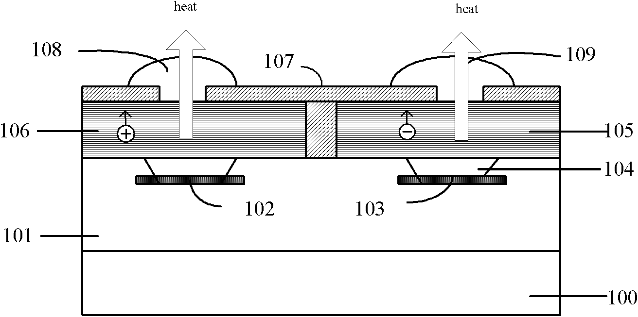
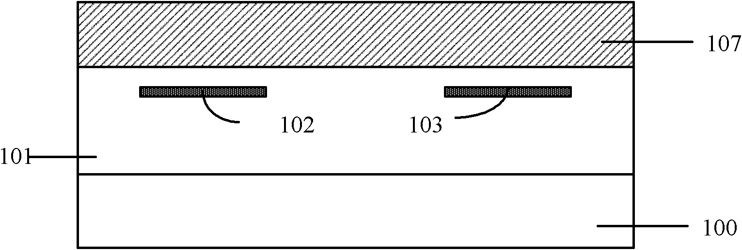
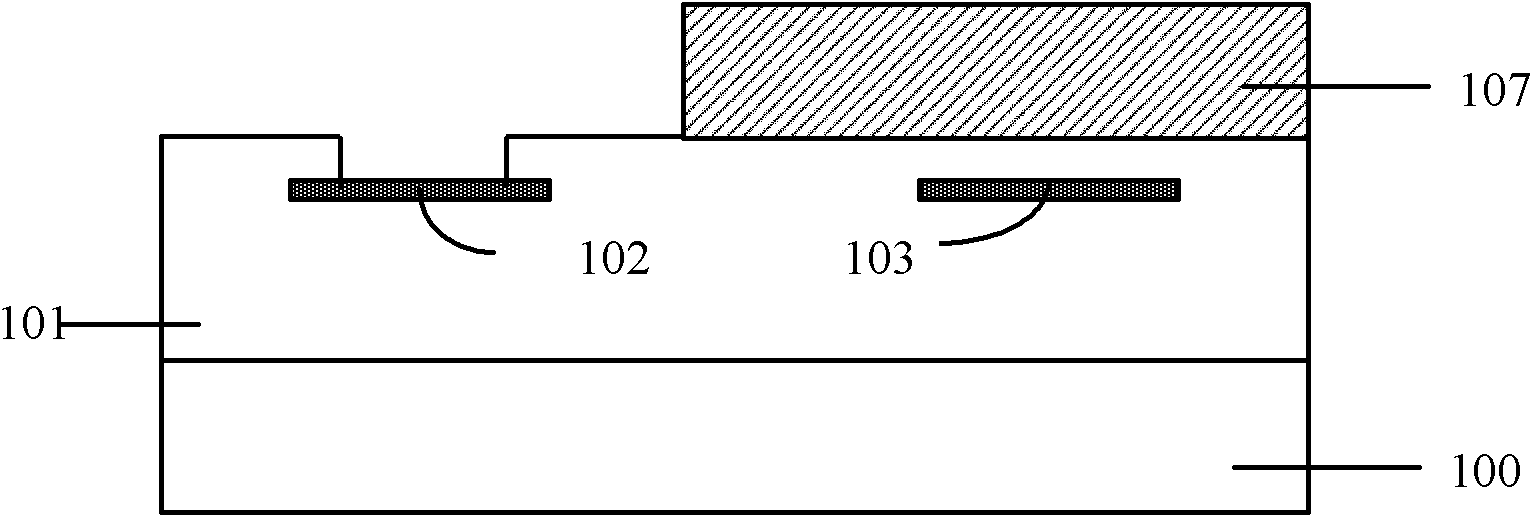
[0022] figure 1 It is a cross-sectional view of the chip thermoelectric heat dissipation structure. The chip includes a substrate 100 and a working area 101, wherein the working layer 101 of the chip includes polysilicon and metal interconnection lines. A P-type superlattice and an N-type superlattice are respectively formed above the chip, and the superlattices are separated by silicon dioxide. ...


PUM


Abstract

The invention provides a cooling structure of a chip, belonging to the field of microelectronics. The cooling structure comprises a P-type superlattice layer and an N-type superlattice layer which are formed on the upper surface of the chip through oxide isolation; a P-type superlattice and an N-type superlattice are isolated by silicon dioxide; the P-type superlattice is electrically connected with a metal layer of the chip through a touch hole, wherein the metal layer of the chip is connected with a low-potential power supply, and meanwhile, a metal layer formed above the P-type superlattice is connected with an external power supply; the N-type superlattice is electrically connected with a metal layer of the chip through a contact hole, wherein the metal layer of the chip is connected with a high-potential power supply, and meanwhile, a metal layer formed above the N-type superlattice is connected with an external power supply; and the potential of the external power supply connected with the P-type superlattice is lower than that of the external power supply connected with the N-type superlattice. By utilizing the characteristics of low thermal conductance and similar phonon localization behaviors of the superlattices, the heat of the chip can be radiated, and meanwhile, the heat from the surrounding environment can be inhibited to transfer to the chip.

Description

technical field [0001] The invention belongs to the field of microelectronics, in particular to a thermoelectric cooling structure, which is mainly used in semiconductor integrated circuit chips. Background technique [0002] With the reduction of the device scale, the increase of the device integration density of a single chip and the increase of the clock frequency lead to the rapid increase of the power consumption of the chip. The sharp increase in power consumption brings about an increase in chip temperature, which will not only degrade the performance of devices and circuits, but also affect the reliability of devices and circuits. Today's high-performance chips generate heat of up to 100 watts per square centimeter. Future chips are likely to generate even higher heat, with chips expected to reach temperatures as high as the surface of the sun without efficient cooling. [0003] The current heat dissipation methods of chips are mainly air-cooled, water-cooled, and ...

Claims


Application Information

Patent Timeline
Patent Type & Authority Applications(China)
IPC IPC(8): H01L23/38H01L29/15
CPCH01L2924/0002H01L23/38H01L23/3738H01L2924/00
Inventor 黄欣张天威黄芊芊秦石强黄如
Owner PEKING UNIV
Why Eureka
Try Eureka