Method for adjusting wafer levels of acoustic coupling resonance filter

An adjustment method and resonator technology, applied in the direction of resonators, waveguide devices, impedance networks, etc., can solve problems such as inability to manufacture, achieve high processing yield, and reduce process crossover or pollution effects

CN102064369BActive Publication Date: 2013-07-17ROFS MICROSYST TIANJIN CO LTD
5 Cites 0 Cited by

Patent Information

Authority / Receiving Office
CN · China
Patent Type
Patents(China)
Current Assignee / Owner
Publication Date
2013-07-17

Smart Images

  • Figure 1
    Figure 1
  • Figure 2
    Figure 2
  • Figure 3
    Figure 3
Patent Text Reader

Abstract

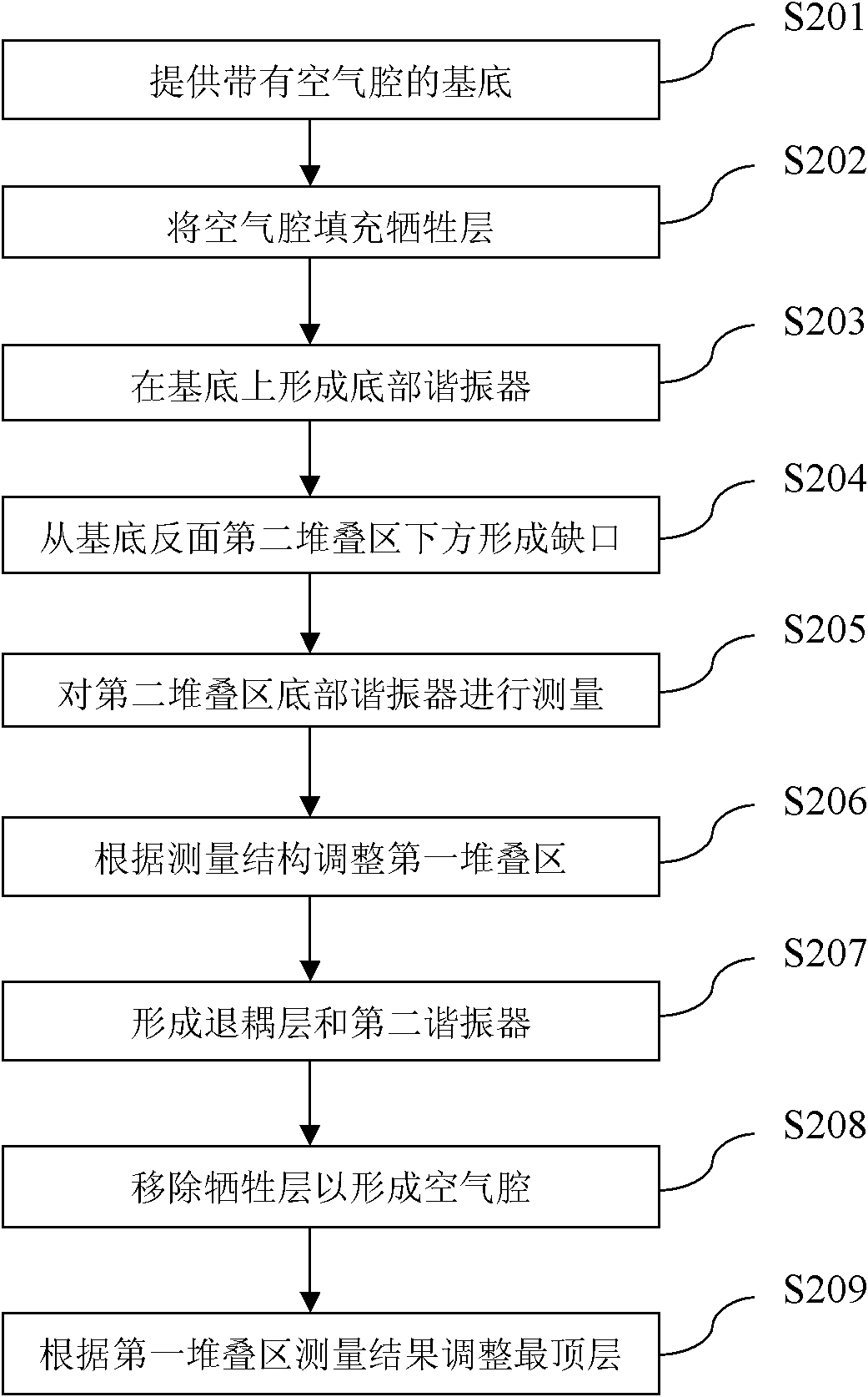
The invention relates to a method for adjusting wafer levels of an acoustic coupling resonance filter. The method comprises the following steps of: providing a substrate of which the partial inside or upper surface is provided with a sacrificial layer; forming a first resonator of a first stack area on the partial sacrificial layer of the substrate; forming a first resonator of a second stack area on the substrate; separating the first resonator of the first stack area from the first resonator of the second stack area; forming an air chamber below the second stack area; measuring the second stack area for the first time; adjusting top electrodes of the first resonator of the first stack area according to the first-time measurement; forming a decoupling layer on the first resonator of the first stack area and the first resonator of the second stack area respectively; forming a second resonator on the decoupling layers of the first stack area and the second stack area respectively; measuring the first stack area or the second stack area for the second time; and adjusting top electrodes of the second resonator of the first stack area according to the result of the second-time measurement so as to realize ideal device performance. By the method, process cross or pollution caused by a release process of the first resonators is reduced to the greatest extent.
Need to check novelty before this filing date? Find Prior Art

Description

technical field

[0001] The invention relates to an acoustic coupling device. More particularly, it relates to a method for wafer-level adjustment of an acoustic coupling resonator filter that applies a correction adjustment process to improve the processing yield of an acoustic coupling device that achieves expected performance. Background technique

[0002] Radio frequency (RF) filters are critical components in any wireless communication system, and as these systems continue to miniaturize, pressure is on filter manufacturers to further reduce filter size without changing device performance. Every day. Handheld device system manufacturers are keenly interested in filter technologies that promise low cost and small size. As the variety of power-hungry applications continues to increase in handheld communication devices, low insertion loss filters are becoming very important to prolong talk time and battery life. Bulk wave (BAW) resonators are known for their high quality...

Examples

Embodiment Construction

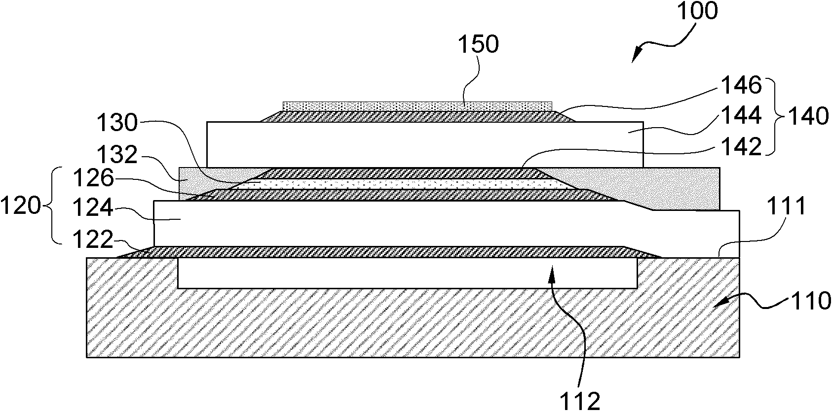
[0101] The wafer-level adjustment method of the acoustic coupling resonator filter of the present invention will be described in detail below with reference to the embodiments and the accompanying drawings.

[0102] The present invention will be described in more detail in the following various forms together with reference to the accompanying drawings, and various embodiments of the present invention will be shown here. The invention exists in many embodiments, however the invention is not limited to the four different example embodiments given here. Moreover, these forms are provided to enable better description and understanding of the present technology, and to fully convey the scope of the present invention to those skilled in the art. The same reference signs refer to the same structural parts.

[0103] In the following, by referring to the attached Figure 1-8 The present invention is described in more detail. In accordance with the purposes of the present invention,...