Matrix dual in-line package (DIP) lead frame, integrated circuit (IC) packages based on frame and production method of IC packages

A lead frame and matrix technology, which is applied in the field of IC chip packages, can solve the problems of high safety risk of DIP manual processing molds, high error rate in the processing process, and low material utilization rate, so as to optimize the production configuration scheme and improve the utilization rate. , the effect of improving utilization

Active Publication Date: 2011-05-25
TIANSHUI HUATIAN TECH
7 Cites 24 Cited by

AI-Extracted Technical Summary

Problems solved by technology

[0004] Since the current single/double row DIP series products are personnel-intensive packaging products, there are low production efficiency, low material utilization rate, hi...

Abstract

The invention provides a matrix dual in-line package (DIP) lead frame, integrated circuit (IC) packages based on the frame and a production method of the IC packages. The matrix DIP lead frame comprises a frame and a plurality of unit frames in the frame, wherein the unit frames are distributed on the frame in a matrix manner and are in odd-numbered lines; the base islands of the adjacent unit frames in the 2n-1 line and the 2n line are connected with the borders of the frame via connecting bars; and the outer lead pins of the adjacent unit frames in the 2n-1 line and the 2n line are arranged in a staggered manner and are connected with the borders of the frame via grids. The invention improves the use ratio of the frame materials, has simple and reasonable structure, has the advantages of low cost, energy conservation and emission reduction and the like, can be widely applied in the fields such as LED tubes, computer interface types, power supply modules, network transformers, DIP switches, pressure sensors, standard logic ICs, large-scale integration (LSI) of memories and the like and is convenient for implementing printed circuit board (PCB) perforating and welding.

Application Domain

Technology Topic

Printed circuit boardDIP switch +11

Image

  • Matrix dual in-line package (DIP) lead frame, integrated circuit (IC) packages based on frame and production method of IC packages
  • Matrix dual in-line package (DIP) lead frame, integrated circuit (IC) packages based on frame and production method of IC packages
  • Matrix dual in-line package (DIP) lead frame, integrated circuit (IC) packages based on frame and production method of IC packages

Examples

  • Experimental program(5)

Example Embodiment

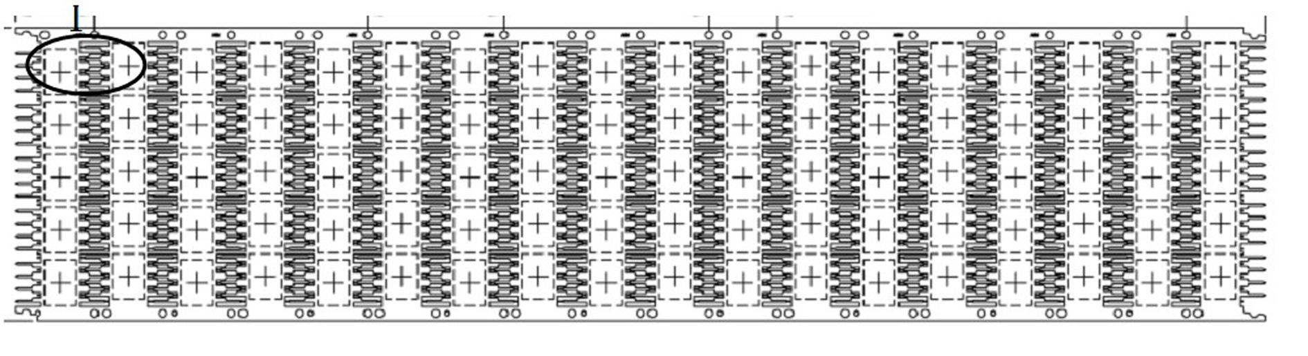
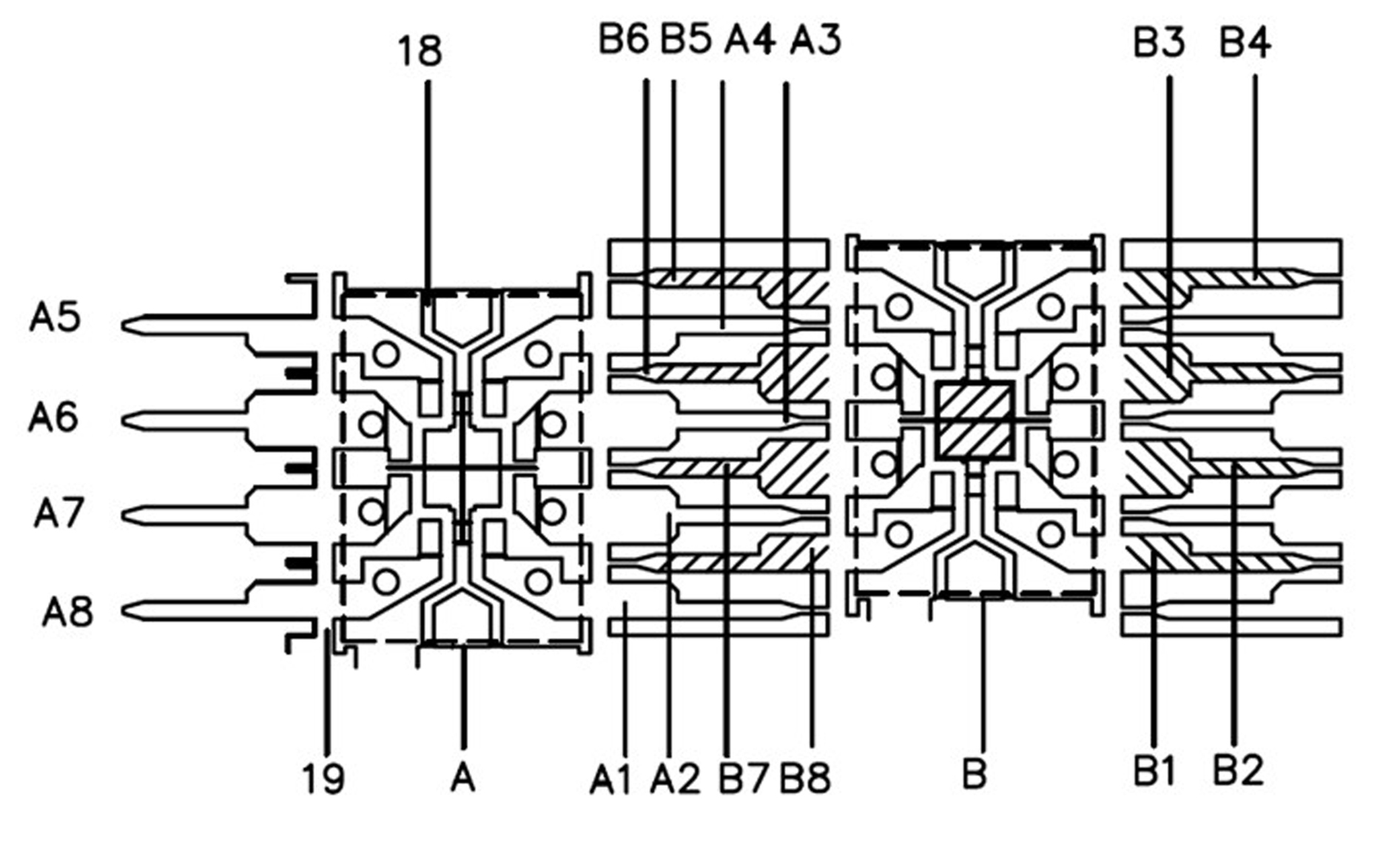
[0041] Embodiment 1, with reference to figure 1 , figure 2 , a single-carrier matrix DIP lead frame, the unit frame is a single-carrier structure and the number of rows is an odd number of rows, wherein the base islands of the adjacent unit frames of the 2n-1th row and the 2nth row are connected to the frame by connecting bars 18 The frames are connected, and the outer leads of the adjacent unit frames in row 2n-1 and row 2n are staggered, and are connected to the frame frames through grid bars 19 . For example: frame A unit and frame B unit are two adjacent unit frames, in which B8 is clamped between A1 and A2 lead pins, A2 is clamped between B8 and B7 lead pins, B7 is clamped between A2 and A3 lead pins A3 is clamped between the pins of B7 and B6, B6 is clamped between the pins of A3 and A4, A4 is clamped between the pins of B6 and B5, and so on.

Example Embodiment

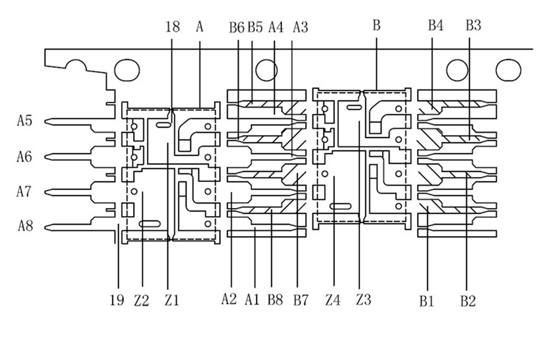
[0042] Embodiment 2, with reference to figure 1 , image 3, a double-carrier matrix DIP lead frame, the unit frame is a double-carrier structure and the number of rows is an odd number of rows, that is, each unit frame has 2 carriers; the pins A7 and A8 of the unit frame A are connected to the carrier Z2, lead The pin A3 is connected to the carrier Z1, the pins B7 and B8 of the adjacent unit frame B are connected to the carrier Z4, and the pin B3 is connected to the carrier Z3; the base island of the adjacent unit frame of the 2n-1 row and the 2n row The connecting bars 18 are connected to the frame frame, and the outer leads of the adjacent unit frames in the 2n-1 row and the 2n row are alternately arranged, and are connected to the frame frame through grid bars 19 . For example: unit frame A and unit frame B are two adjacent package units, in which B8 is clamped between the pins of A1 and A2, A2 is clamped between the pins of B8 and B7, and B7 is clamped between the pins of A2 and A3 A3 is clamped between the pins of B7 and B6, B6 is clamped between the pins of A3 and A4, A4 is clamped between the pins of B6 and B5, and so on. And according to the needs, there are more special-shaped structural frames.

Example Embodiment

[0043] Embodiment 3, with reference to figure 1 , figure 2 , Figure 4 , a dual-chip IC package based on the unit frame of embodiment 1, comprising a carrier 1 on the unit frame, first and second IC chips 11, 12 are placed in parallel on the carrier 1 of the unit frame, the first On the pads on the IC chip 11 and the second IC chip 12, respectively pre-plant a gold wire or copper wire solder ball 10, and then use gold wire or copper wire on the gold wire or copper wire ball 10 of the first IC chip 11 Stacking gold wires or copper wire bonding balls, arching wire drawing arcs stacking gold or copper bonding balls on the gold or copper balls of the pads on the second IC chip 12 to form bonding balls 20, the bonding balls 20 make The first and second IC chips 11 and 12 are connected; the outer pads of the first and second IC chips 11 and 12 are connected to the inner pins 4 of the unit frame through copper or gold bonding wires 5 bonding; finally, plastic packaging The body 6 completely covers the first and second IC chips 11, 12, bonding alloys or copper wires 5, 9, gold or copper balls 10, bonding balls 20 and lead pins 4 of the unit frame to form a whole circuit.

PUM

no PUM

Description & Claims & Application Information

We can also present the details of the Description, Claims and Application information to help users get a comprehensive understanding of the technical details of the patent, such as background art, summary of invention, brief description of drawings, description of embodiments, and other original content. On the other hand, users can also determine the specific scope of protection of the technology through the list of claims; as well as understand the changes in the life cycle of the technology with the presentation of the patent timeline. Login to view more.

Similar technology patents

Classification and recommendation of technical efficacy words

  • Improve production efficiency and product quality
  • Reduce error rate

Uplink carrier scheduling method for carrier aggregation communication system, base station and user equipment

ActiveCN101835191AReasonable schedulingReduce error rateWireless communicationCarrier signalSignal-to-interference-plus-noise ratio
Owner:北京万海云科技有限公司
Why Eureka
Try Eureka