
Method for forming stack gate of CMOS (Complementary Metal-Oxide-Semiconductor) device and stack gate sturcture

A technology of MOS devices and gate dielectrics, applied in semiconductor devices, electrical components, transistors, etc., can solve the problems of carrier mobility reduction, device performance degradation, large scattering of channel carriers, etc., and achieve improved channel migration rate, reduce gate leakage current, and adjust the effect of threshold voltage

Inactive Publication Date: 2011-05-25
INST OF MICROELECTRONICS CHINESE ACAD OF SCI
View PDF0 Cites 3 Cited by
  • Summary
  • Abstract
  • Description
  • Claims
  • Application Information

AI Technical Summary

Problems solved by technology

In addition, some elements will form a certain amount of charges or defects when they are close to the channel of the MOS device, which will greatly scatter the channel carriers, resulting in a decrease in carrier mobility, resulting in poor device performance. Degradation, such as N, Al, La, etc.

Method used


Image

  • Method for forming stack gate of CMOS (Complementary Metal-Oxide-Semiconductor) device and stack gate sturcture
  • Method for forming stack gate of CMOS (Complementary Metal-Oxide-Semiconductor) device and stack gate sturcture
  • Method for forming stack gate of CMOS (Complementary Metal-Oxide-Semiconductor) device and stack gate sturcture

Examples


Embodiment 1

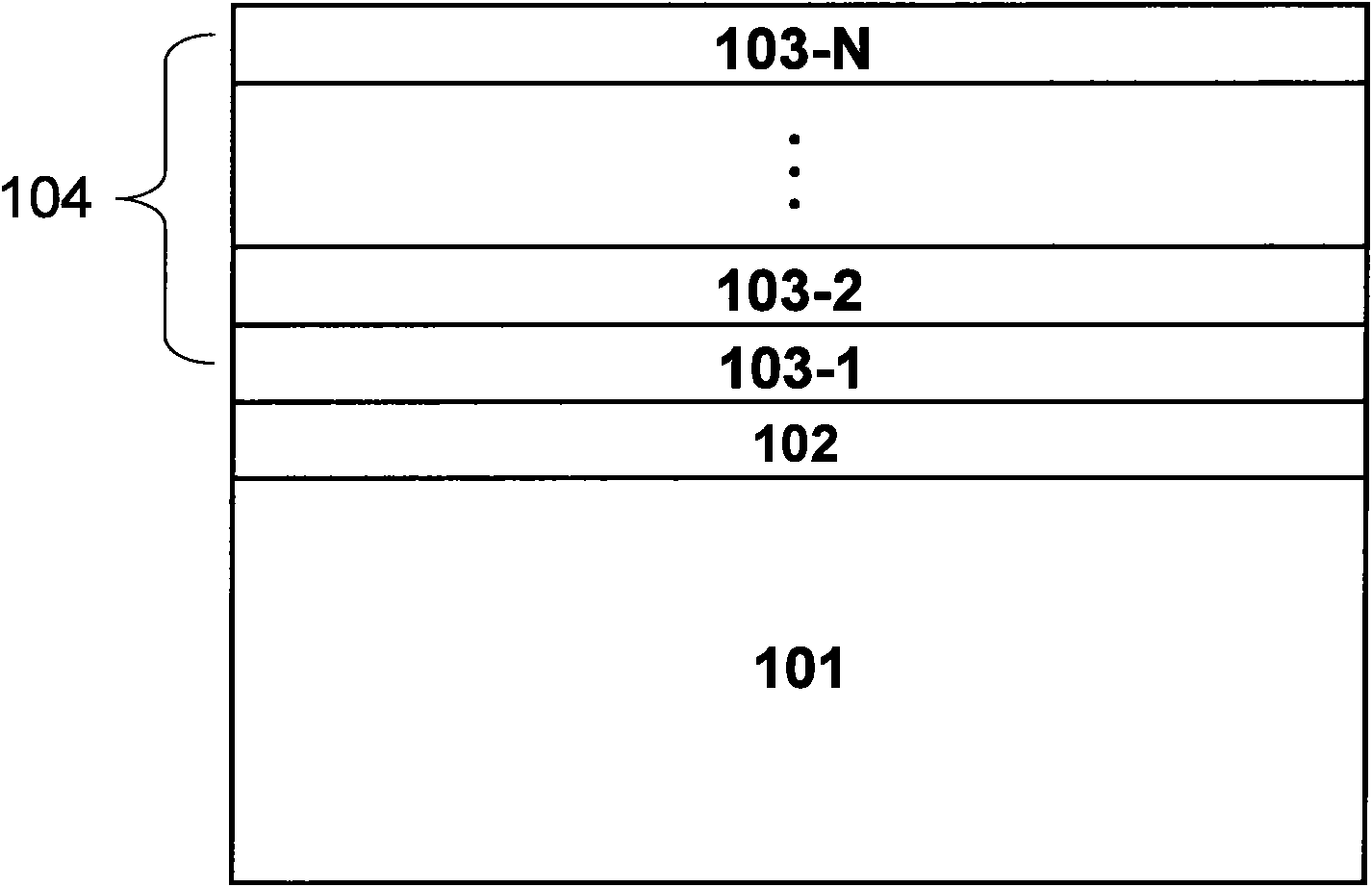
[0027] Such as Figure 2-5 As shown, it is a schematic diagram of forming the gate stack structure of the present invention in Embodiment 1 of the present invention. In this embodiment, the multi-layer insulating film is a three-layer film with the same thickness and different atomic percentages. Of course, in other embodiments, the insulating film It can also be different, including the following steps:

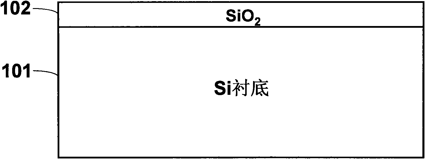
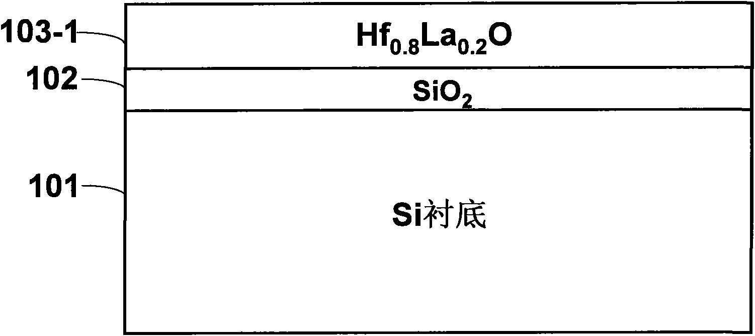
[0028] Step 1: If figure 2 As shown, the interface layer film 102 is grown on the silicon substrate 101 that has been processed in the early stage, and its thickness is about 0.5nm. In the embodiment of the present invention, the interface layer film 102 is SiO 2 interface layer film. In this embodiment, the interface layer film 102 is made of SiO 2 This is described as an example. In other embodiments, other materials mentioned above can be selected as the interface layer film 102 .

[0029] Step 2: If image 3 shown in SiO 2 ALD technology is used to grow the first ...

Embodiment 2

[0037] Such as Figure 6-11 As shown, it is a schematic diagram of forming the gate stack structure of the present invention according to Embodiment 2 of the present invention, which includes the following steps:

[0038] Step 1: grow a 0.5nm-thick interface layer film 102 on the silicon substrate 101 that has been processed in the previous stage, such as Image 6 As shown, in this embodiment the interface layer film 102 is SiO 2 . In this embodiment, the interface layer film 102 is made of SiO 2 This is described as an example. In other embodiments, other materials mentioned above can be selected as the interface layer film 102 .

[0039] Step 2: If Image 6 As shown, the first layer of insulating film 103-1 is grown by ALD technology on the interface layer film 102, and its thickness is about 1nm. In this embodiment, the first layer of insulating film 103-1 is HfO 2 film.

[0040] Step 3: If Figure 7 As shown, the second layer of insulating film 103-2 is grown by ALD...

Embodiment 3

[0050] Such as Figure 12-15 As shown, it is a schematic diagram of forming the gate stack structure of the present invention according to Embodiment 3 of the present invention, which includes the following steps:

[0051] Step 1: If Figure 12 As shown, a layer of 0.3nm thick HfO is grown by ALD technology on the silicon substrate 101 that has been processed in the early stage. 2 Film 102.

[0052] Step 2: In a nitrogen atmosphere, take the first annealing treatment of the structure at 700°C for 20s to form HfSiO x interface layer film 102, Figure 13 shown.

[0053] Step 3: If Figure 13 shown, in HfSiO x The first layer of insulating film 103-1 is grown on the interface layer film 102 by ALD technology, and its thickness is about 0.5nm. In this embodiment, the first layer of insulating film 103-1 is a HfLaON film.

[0054] Step 4: If Figure 14 As shown, the second layer of insulating film 103-2 is grown by ALD technology on the first layer of insulating film 103-1,...


PUM

PropertyMeasurementUnit
Thicknessaaaaaaaaaa
Thicknessaaaaaaaaaa
Thicknessaaaaaaaaaa

Abstract

The invention provides a gate medium structure of an MOS ( Metal-Oxide-Semiconductor) device, which comprises a boundary layer film formed on the surface of a semiconductor substrate and at least two layers of insulating films formed on the surface of the boundary layer film, wherein each of the at least two layers of insulating films has element components and concentrations, which are different from that of other adjacent insulating films, the boundary layer film and the at least two layers of insulating films are processed by an optimized annealing process, and the optimized annealing process is related to the element components and the concentrations of the boundary layer film and the at least two layers of insulating films so as to realize ideal distribution of the element components and the concentrations. In the invention, the gate medium structure of the MOS device is formed by depositing multiple layers of different material components or different concentrations of films in a certain order, and then, the ideal distribution of all element components and the concentrations in the gate medium structure is realized by the optimized annealing process.

Description

technical field [0001] The invention relates to a method and structure for forming a semiconductor device, in particular to a method for forming a stacked gate dielectric of a CMOS device and its structure. Background technique [0002] For decades in the development of microelectronics technology, logic chip manufacturers have been using SiO2 when manufacturing MOS devices. 2 As the gate dielectric, heavily doped polysilicon is used as the gate electrode material. However, as feature sizes continue to shrink, SiO in MOS transistors 2 The gate dielectric is approaching its limit. For example, in a 65nm process, SiO 2 The thickness of the gate has been reduced to 1.2 nanometers, which is about 5 silicon atomic layers thick. If it continues to shrink, the leakage current and power consumption will increase sharply. At the same time, problems such as the diffusion of doped boron atoms caused by the polysilicon gate electrode, the polysilicon depletion effect, and the excess...

Claims


Application Information

Patent Timeline
IPC IPC(8): H01L29/51H01L27/092H01L21/28
Inventor 陈世杰王文武王晓磊韩锴
Owner INST OF MICROELECTRONICS CHINESE ACAD OF SCI
Learn More