Thin film solar cell and manufacturing method thereof
A solar cell and manufacturing method technology, applied in circuits, photovoltaic power generation, electrical components, etc., can solve the problems of short circuit, thin film solar cell yield, reliability decline, etc., to prevent short circuit and leakage, good light capture effect, power generation The effect of fewer layer defects
- Summary
- Abstract
- Description
- Claims
- Application Information
AI Technical Summary
Problems solved by technology
Method used
Image

Examples
Embodiment approach 1
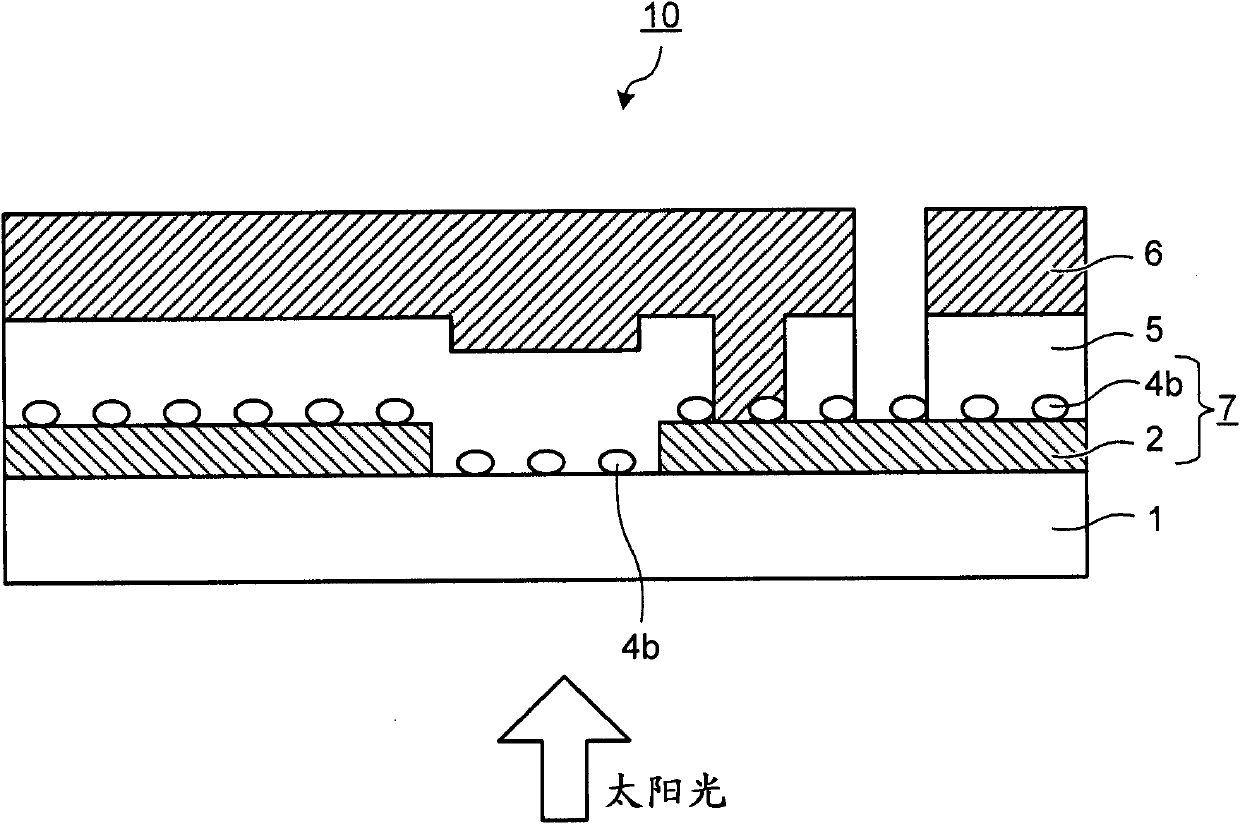
[0039] figure 1It is a cross-sectional view showing a schematic structure of the thin-film solar cell 10 according to Embodiment 1 of the present invention. The thin film solar cell 10 includes: a transparent insulating substrate 1, a first transparent conductive film (transparent electrode layer) 2 formed on the transparent insulating substrate 1 and serving as a first electrode layer, a first transparent conductive film (transparent electrode layer) 2 formed on the transparent insulating substrate 1 and the first transparent conductive film 2 The conductive oxide light scatterer 4b on the conductive oxide light scatterer 4b, the first power generation layer 5 formed on the conductive oxide light scatterer 4b, and the back electrode layer 6 formed on the first power generation layer 5 and serving as the second electrode layer.
[0040] In addition, the first power generation layer 5 is composed of at least two or more layers, and in this embodiment includes a P-type amorphous...
Embodiment approach 2
[0069] Figure 5 It is a cross-sectional view showing a schematic structure of a tandem thin-film solar cell 20 according to Embodiment 2 of the present invention. The tandem thin-film solar cell 20 related to the second embodiment is a modified example of the thin-film solar cell 11 of the first embodiment, and includes a transparent insulating substrate 1, a first transparent conductive film (transparent electrode layer) 2, a conductive oxide light-scattering Body 4b, first power generation layer 5, second power generation layer 8, conductive oxide light scatterer 4c, and back electrode layer 6. exist Figure 5 In , for the same components as those of the thin-film solar cells 10 and 11 related to Embodiment 1, the marks and figure 1 as well as image 3 same symbols, and their descriptions are omitted.
[0070] The thin film solar cell 20 differs from the thin film solar cell 11 of Embodiment 1 in that a conductive oxide light scatterer 4 c is formed as a conductive ligh...
Embodiment approach 3
[0094] Figure 8-1 It is a cross-sectional view showing a schematic structure of a thin-film solar cell 30 according to Embodiment 3 of the present invention. The thin-film solar cell 30 related to Embodiment 3 is a modified example of the thin-film solar cell 10 in Embodiment 1. Like the thin-film solar cell 10, it includes: a transparent insulating substrate 1, a first transparent conductive film (transparent electrode layer) 2, a conductive Oxide light scatterer 4 b , first power generation layer 5 , and back electrode layer 6 . exist Figure 8-1 In , for the same components as those of the thin-film solar cell 10 related to Embodiment 1, the marks and figure 1 The same symbols are used and their explanations are omitted.
[0095] The difference between the thin-film solar cell 30 and the thin-film solar cell 10 of Embodiment 1 is that the separated first transparent conductive layer on the surface of the first transparent conductive film (transparent electrode layer) 2 ...
PUM
| Property | Measurement | Unit |
|---|---|---|
| thickness | aaaaa | aaaaa |
| thickness | aaaaa | aaaaa |
| thickness | aaaaa | aaaaa |
Abstract
Description
Claims
Application Information
 - R&D
- Intellectual Property
- Life Sciences
- Materials
- Tech Scout
- Unparalleled Data Quality
- Higher Quality Content
- 60% Fewer Hallucinations
Browse by: Latest US Patents, China's latest patents, Technical Efficacy Thesaurus, Application Domain, Technology Topic, Popular Technical Reports.
© 2025 PatSnap. All rights reserved.Legal|Privacy policy|Modern Slavery Act Transparency Statement|Sitemap|About US| Contact US: help@patsnap.com