Supercharge Your Innovation With Domain-Expert AI Agents!

A wafer manufacturing device for a solar battery cell and a wafer manufacturing method using the same

A solar cell and manufacturing device technology, applied in electrical components, circuits, photovoltaic power generation, etc., can solve problems such as difficulty in increasing solar power generation efficiency and increase in operating hours, so as to improve power generation efficiency, reduce popularization costs, and minimize manufacturing costs effect

Inactive Publication Date: 2013-05-29
CITY ENVIRONMENT ENG
View PDF8 Cites 0 Cited by
  • Summary
  • Abstract
  • Description
  • Claims
  • Application Information

AI Technical Summary

Problems solved by technology

[0010] However, as mentioned above, the wafer preparation process for manufacturing conventional solar cells involves the preparation of a cylindrical silicon single crystal ingot, cutting and processing, and thus there is a problem of increased man-hours.
[0011] Furthermore, the power generation efficiency of solar cells is influenced by the density and purity of silicon, but in conventional methods, there is a limit to the improvement of wafer density, so there is a problem that it is difficult to increase solar power generation efficiency

Method used


Image

  • A wafer manufacturing device for a solar battery cell and a wafer manufacturing method using the same
  • A wafer manufacturing device for a solar battery cell and a wafer manufacturing method using the same
  • A wafer manufacturing device for a solar battery cell and a wafer manufacturing method using the same

Examples


Embodiment Construction

[0021] Hereinafter, preferred embodiments of the present invention will be described in further detail based on the drawings.

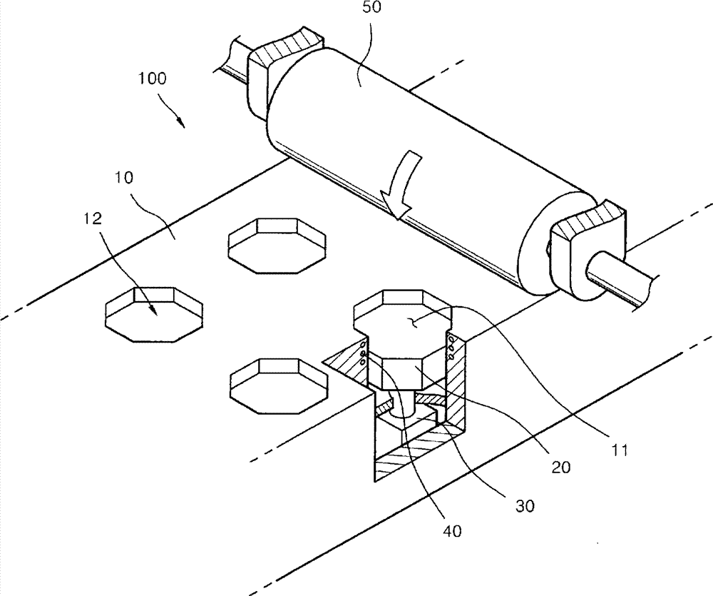
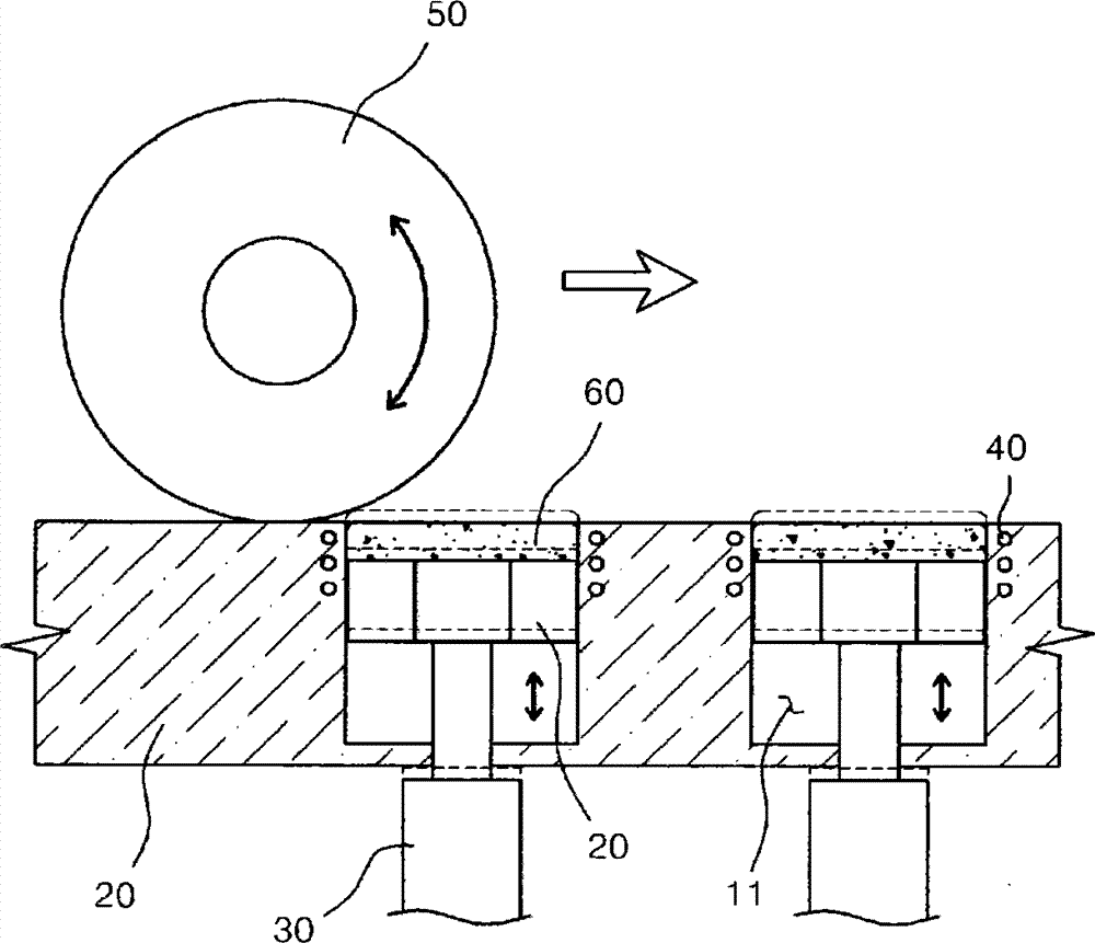
[0022] refer to figure 1 and figure 2 A solar cell wafer manufacturing apparatus 100 (hereinafter referred to as “wafer manufacturing apparatus”) of the present invention includes a mold 10 , a lifting member 20 , a driver 30 , a heater 40 , and a pressurizing device.

[0023] The mold 10 is formed with a casting mold 12 corresponding to the wafer shape of the solar cell unit on the upper surface, and the cross section of the wafer in this embodiment is hexagonal, so a hexagonal filling groove is formed from the upper surface of the mold 10 to the bottom 11. The lifting member 20 is provided in the filling tank 11 so as to be able to move up and down freely, thereby forming a filling space filled with the molten wafer raw material 60 , that is, a mold 12 .

[0024] Inside the mold 10 is provided an installation space where the driver 30 for raising...


PUM


Abstract

The present invention relates to a wafer making device for a solar battery cell having a high density silicon wafer for increasing generation efficiency, and a wafer manufacturing method using the same. The wafer making device comprises: a mold in the shape of a wafer for manufacturing a solar battery cell; a lift installed on said mold to elevate dissolved wafer raw material after the mold is filled; an actuator for elevating and lowering said lift; and a device for pressing the wafer material filling said mold to compress it during a hardening process thereby increasing the density of the wafer. The present invention significantly decreases supply costs for solar energy generation because it minimizes costs for solar battery cell manufacture, and it also increases generation efficiency.

Description

technical field [0001] The present invention relates to a wafer manufacturing device for solar cells and a wafer manufacturing method using the device, in particular to a wafer manufacturing device for solar cells with a higher density of silicon wafers and a wafer manufacturing method using the device method to improve power generation efficiency. Background technique [0002] Generally, solar cells can be classified into crystalline silicon solar cells, amorphous (amorphous) silicon solar cells, and compound semiconductor solar cells based on substrate materials. In addition, crystalline silicon solar cells can be divided into monocrystalline silicon solar cells and polycrystalline silicon solar cells. [0003] For solar cells, conversion efficiency is the most important characteristic. Among solar cells, compound semiconductor solar cells have relatively high conversion efficiency, which is close to 25%. However, since compound semiconductor solar cells are difficult t...

Claims


Application Information

Patent Timeline
Patent Type & Authority Patents(China)
IPC IPC(8): H01L31/04
CPCH01L31/18Y02E10/50H01L31/036H01L31/04Y02E10/547
Inventor 孔锺炫
Owner CITY ENVIRONMENT ENG
Features
  • R&D
  • Intellectual Property
  • Life Sciences
  • Materials
  • Tech Scout
  • Unparalleled Data Quality
  • Higher Quality Content
  • 60% Fewer Hallucinations
Learn More