

Organic semiconductor visible light photocatalyst with membrane structure and preparation method and application thereof
A technology of organic semiconductors and photocatalysts, applied in organic compound/hydride/coordination complex catalysts, physical/chemical process catalysts, chemical instruments and methods, etc., to reduce costs, increase separation efficiency, and improve utilization.
- Summary
- Abstract
- Description
- Claims
- Application Information
AI Technical Summary
Problems solved by technology
Method used
Image

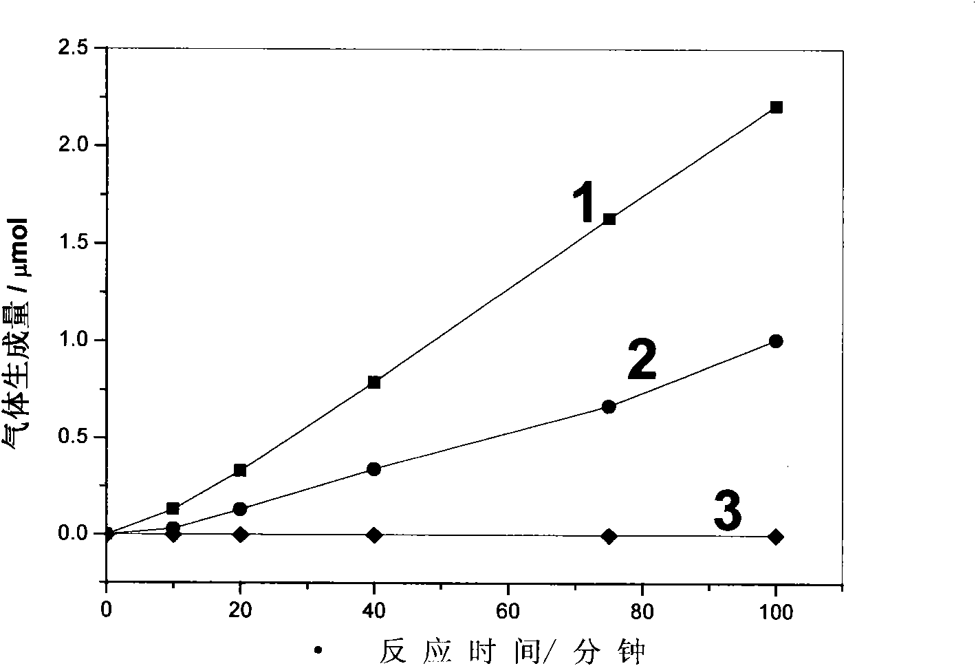
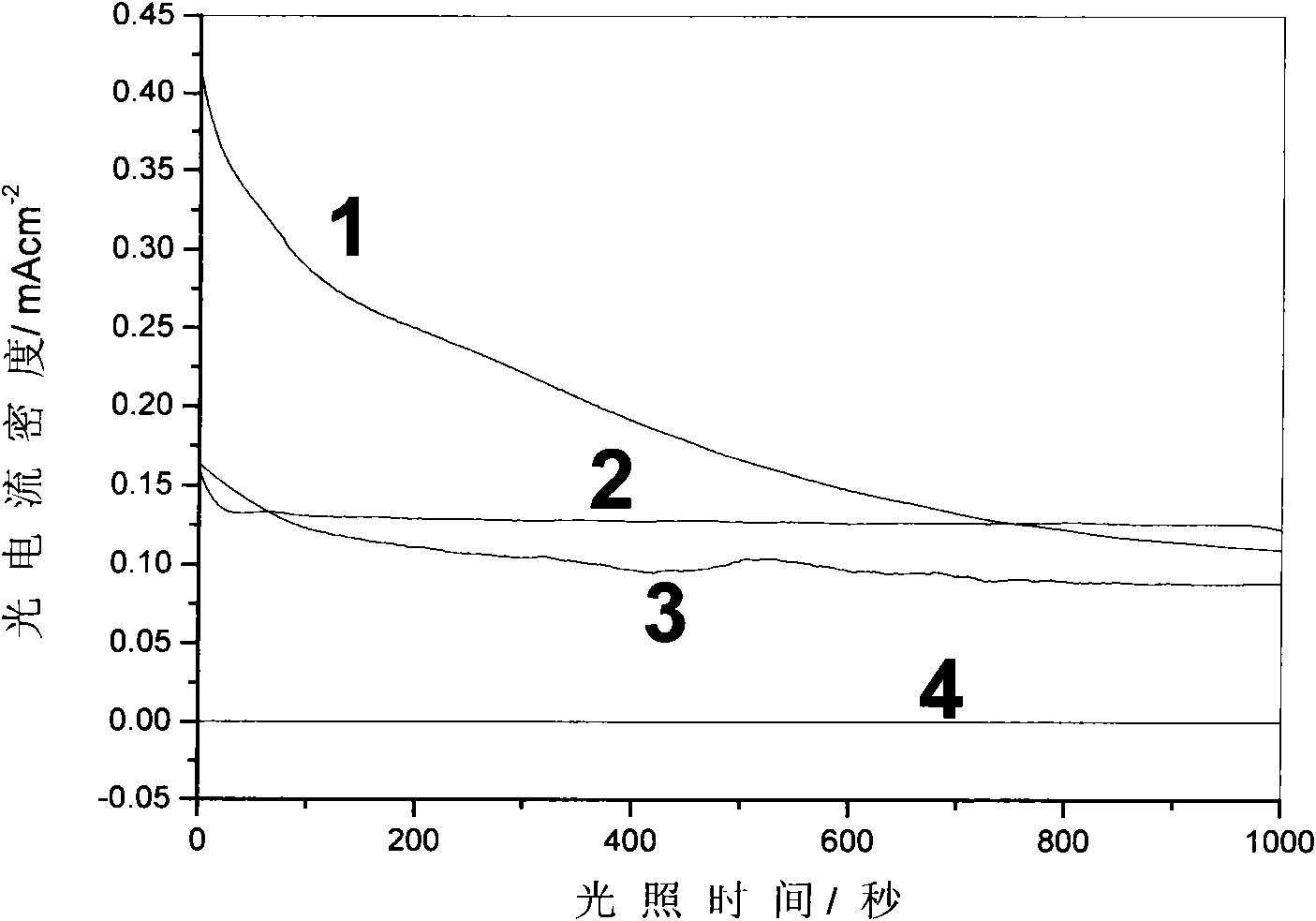
Examples
Embodiment 1
[0041]
[0042] Perylenetetracarboxylic dianhydride [6,6]-phenyl-C 61 Methyl butyrate, Me is methyl
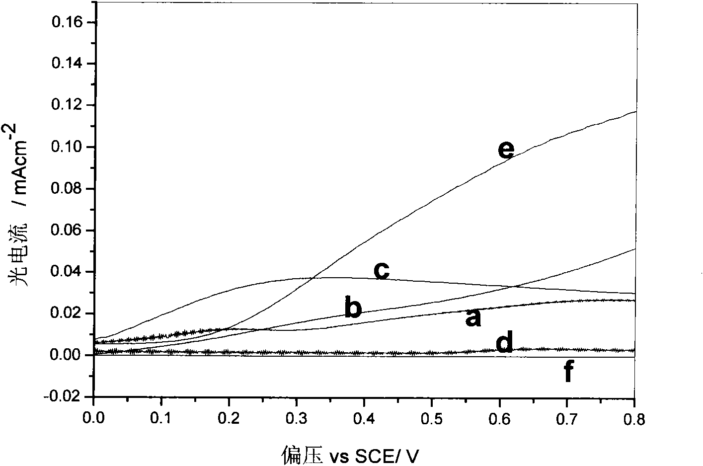
[0043] Utilize above-mentioned perylenetetracarboxylic dianhydride and [6,6]-phenyl-C 61 Methyl butyrate was used to prepare five different membranes from membranes a to d. The specific methods are as follows:
[0044] Preparation of membrane a:
[0045] (1) A quartz container with perylenetetracarboxylic dianhydride is placed in a crucible of a vacuum evaporation apparatus, and a 4×2cm conductive glass ITO is placed above the cavity of the vacuum evaporation apparatus, and then vacuumized to 1×10 -5 ~4×10 -5 Pa;
[0046] (2). On the vacuum vapor deposition apparatus of adjustment step (1), it is 1.5~1.8A to control the heating of the crucible that is loaded with perylene tetracarboxylic dianhydride to be 1.5~1.8A, heat perylene tetracarboxylic dianhydride, make perylene tetracarboxylic dianhydride Evaporate on the conductive glass ITO, and coat a layer of perylene te...
Embodiment 2
[0075] (1) Perylene tetracarboxylic dianhydride and [6,6]-phenyl-C 61 The two quartz containers of methyl butyrate are placed in the two crucibles of the same vacuum evaporator, and a 4×2 cm conductive glass ITO is placed above the cavity of the vacuum evaporator, and then vacuumed to 1×10 -5 ~4×10 -5 Pa;
[0076] (2). On the vacuum vapor deposition apparatus of adjustment step (1), it is 1.5A to control the heating current of the crucible loaded with perylene tetracarboxylic dianhydride to heat perylene tetracarboxylic dianhydride so that perylene tetracarboxylic dianhydride is vapor-deposited On the conductive glass ITO, plate a layer of perylene tetracarboxylic dianhydride film on the conductive glass ITO; at the same time, closely observe the film thickness monitor on the vacuum evaporation instrument, when the thickness of the perylene tetracarboxylic dianhydride film reaches 10 Stop coating when nanometer is reached;
[0077] (3). No need to take it out, and then cont...
Embodiment 3
[0081] (1) Perylene tetracarboxylic dianhydride and [6,6]-phenyl-C 61 The two quartz containers of methyl butyrate are placed in the two crucibles of the same vacuum evaporator, and a 4×2 cm conductive glass ITO is placed above the cavity of the vacuum evaporator, and then vacuumed to 1×10 -5 ~4×10 -5 Pa;
[0082] (2). On the vacuum vapor deposition apparatus of adjustment step (1), it is 1.8A to control the heating current of the crucible loaded with perylene tetracarboxylic dianhydride to heat perylene tetracarboxylic dianhydride so that perylene tetracarboxylic dianhydride is vapor-deposited On the conductive glass ITO, plate a layer of perylene tetracarboxylic dianhydride film on the conductive glass ITO; at the same time, closely observe the film thickness monitor on the vacuum evaporation instrument, when the thickness of the perylene tetracarboxylic dianhydride film reaches 30 Stop coating when nanometer is reached;
[0083] (3). No need to take it out, and then adju...
PUM
| Property | Measurement | Unit |
|---|---|---|
| thickness | aaaaa | aaaaa |
| thickness | aaaaa | aaaaa |
| band gap | aaaaa | aaaaa |
Abstract
Description
Claims
Application Information