Electrochemical sensor chip based on digital microfluidic technology

A technology of sensor chips and digital microfluidics, applied in the field of microanalysis, can solve problems such as inability to realize chip integration

Inactive Publication Date: 2011-06-15
FUDAN UNIV
View PDF9 Cites 29 Cited by
  • Summary
  • Abstract
  • Description
  • Claims
  • Application Information

AI Technical Summary

Problems solved by technology

However, because optical detection requires a huge optical system, the existing techn

Method used


Image

  • Electrochemical sensor chip based on digital microfluidic technology
  • Electrochemical sensor chip based on digital microfluidic technology
  • Electrochemical sensor chip based on digital microfluidic technology

Examples


Embodiment Construction

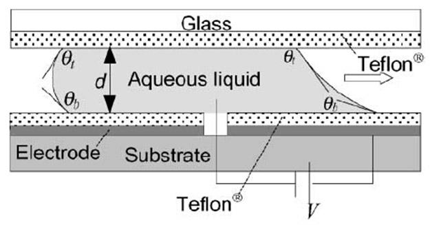
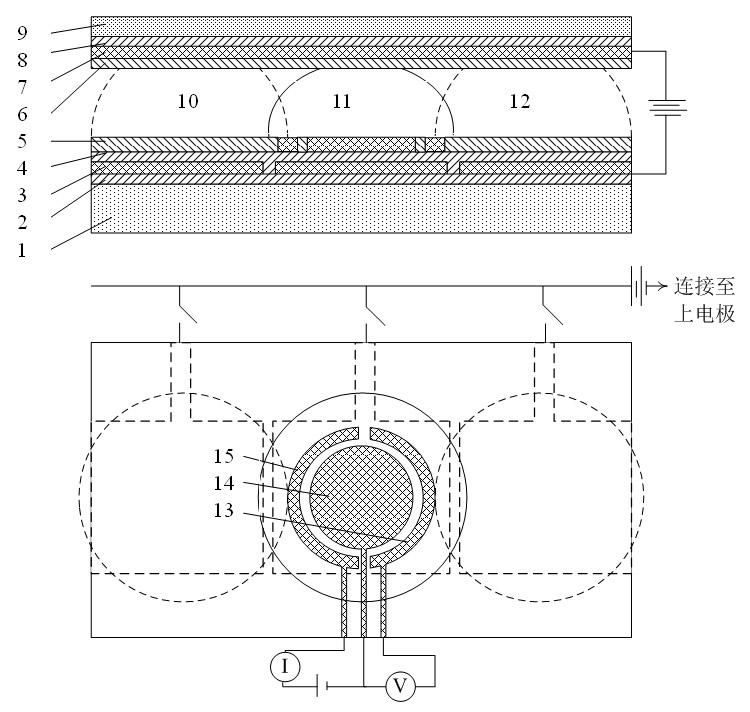
[0028] according to figure 2 Shown, the concrete implementation step of the present invention is as follows:

[0029] bottom layer

[0030] 1) Preparation of Substrate 1.

[0031] The substrate 1 can be any material, including a flexible substrate. If the substrate is a conductive material, an insulating layer 2 should be deposited first, and the process of depositing the insulating layer can be thermal oxidation, chemical vapor deposition CVD or physical vapor deposition PVD and other processes. For example, if the substrate is made of silicon, an insulating layer of silicon dioxide can be used.

[0032] 2) Deposition and patterning of the electrode layer 3 .

[0033] The electrode 3 can be metal, conductive polymer or conductive oxide, etc., and the electrode layer is deposited by spin coating annealing, physical sputtering or evaporation process. Patterning can use a) etching after photolithography (dry or wet), or lift-off process; b) hard mask combined with physical...


PUM


Abstract

The invention belongs to the technical field of micro analysis, in particular to an electrochemical sensor chip based on the digital microfluidic technology. The sensor chip comprises a digital microfluidic device and a three-electrode electrochemical device, wherein the three-electrode electrochemical device is stacked on the digital microfluidic device; the digital microfluidic device comprises a bottom layer and an upper cover, wherein the bottom layer comprises a first substrate, a first insulating layer, a first electrode layer, a second insulating layer and a first drainage layer in sequence from bottom to top; the upper cover comprises a second drainage layer, a second electrode layer, a third insulating layer and a second substrate in sequence from bottom to top; when the first substrate and the second substrate are made of insulating materials, the first insulating layer and the third insulating layer are dispensed; three electrodes include a counter electrode, a working electrode and a reference electrode; and the three electrodes and the first drainage layer are positioned on the same plane and surrounded but not covered by the first drainage layer. The electrochemical sensor chip can realize the delivery and the online detection of various required liquid samples.

Description

technical field [0001] The invention belongs to the technical field of microanalysis, and in particular relates to an electrochemical sensor chip based on digital microfluidic technology. Background technique [0002] In the past ten years, the concept of "total microanalysis system" (μ-TAS) or "lab-on-a-chip" (Lab-on-a-chip) has been rapidly developed and realized, which uses microfabrication and integration technology Combining various analysis and detection principles, the miniature analytical instrument has the advantages of small size, low power consumption, high sensitivity, and portability. It can be widely used in biological, medical and chemical detection. It is used in national security, immune detection, environmental protection, Food hygiene, genetic screening, disease diagnosis and other fields have application potential. [0003] Regardless of the object of its analysis and detection, the structural composition of the "full micro-analysis system" or "lab-on-a-...

Claims


Application Information

Patent Timeline
IPC IPC(8): G01N27/416
Inventor 周嘉杨盛曾祥宇
Owner FUDAN UNIV
Why Eureka
Try Eureka