Silicon drift detector with curved surface structure
A silicon drift detector and curved surface technology, applied in semiconductor devices, radiation intensity measurement, sustainable manufacturing/processing, etc. Multiple applications, avoid punch-through effect, improve stability effect
- Summary
- Abstract
- Description
- Claims
- Application Information
AI Technical Summary
Problems solved by technology
Method used
Image

Examples
Embodiment Construction
[0043] The present invention will be further described below through specific embodiments in conjunction with the accompanying drawings.
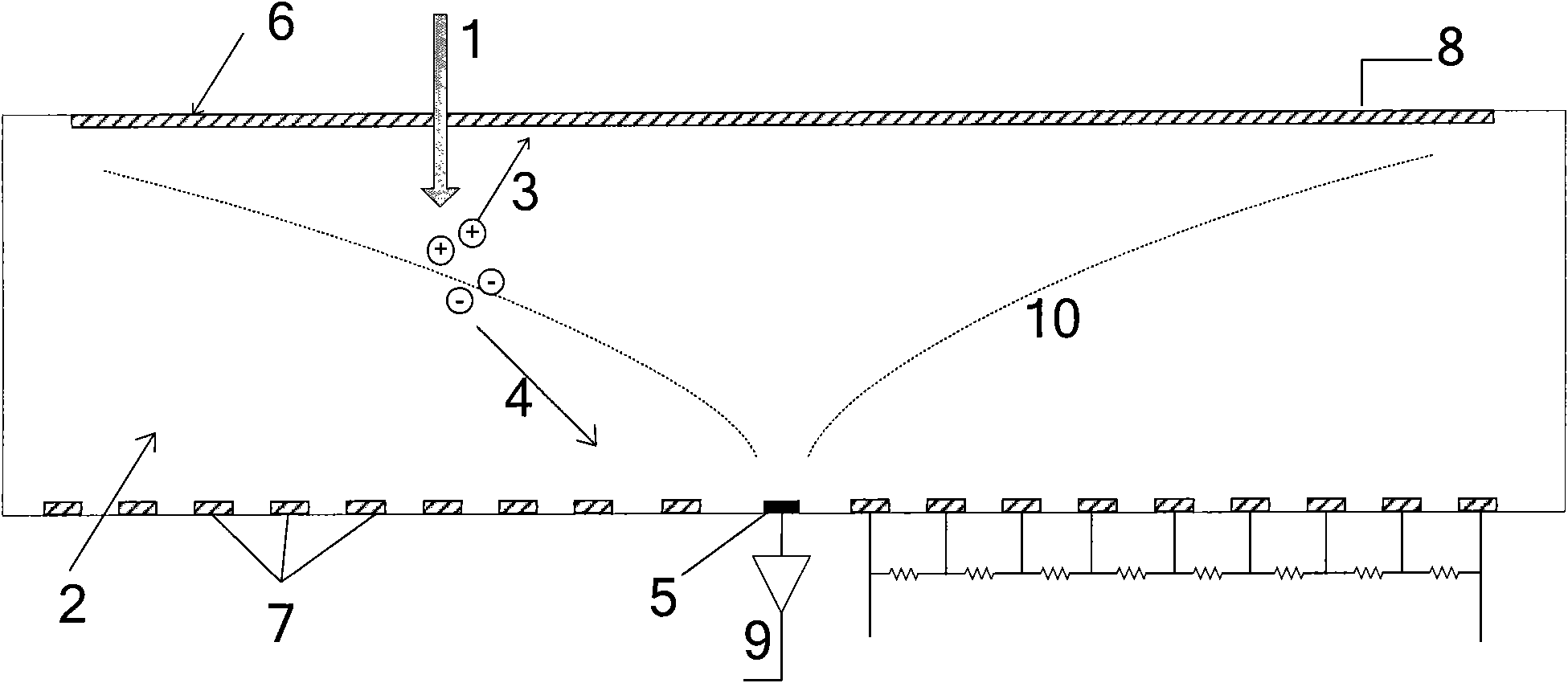
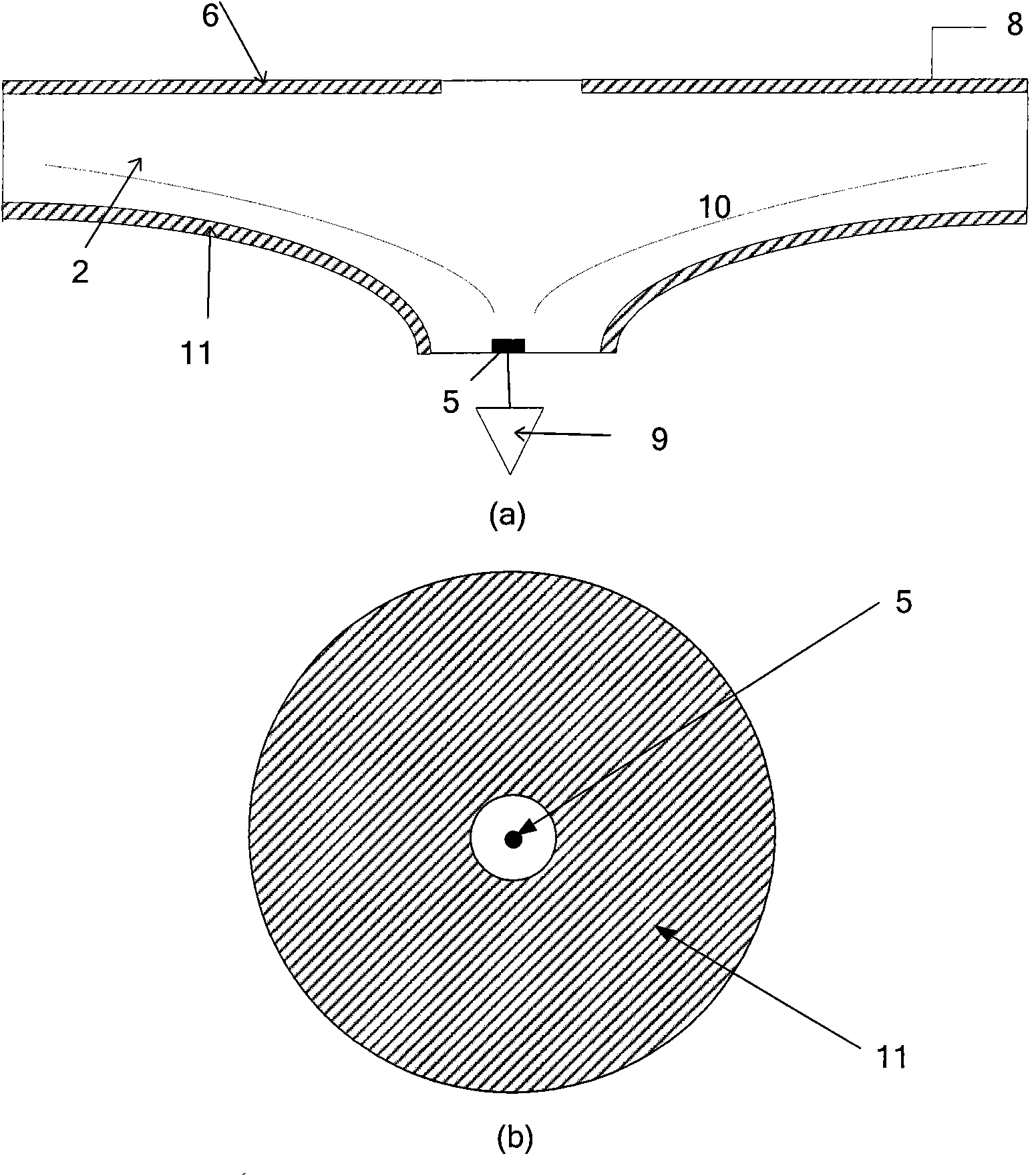
[0044] The following examples are intended to be manufactured by a specific manufacturing method figure 2 A silicon drift detector with a curved surface structure is shown.
[0045] Concrete manufacturing method comprises the following steps:
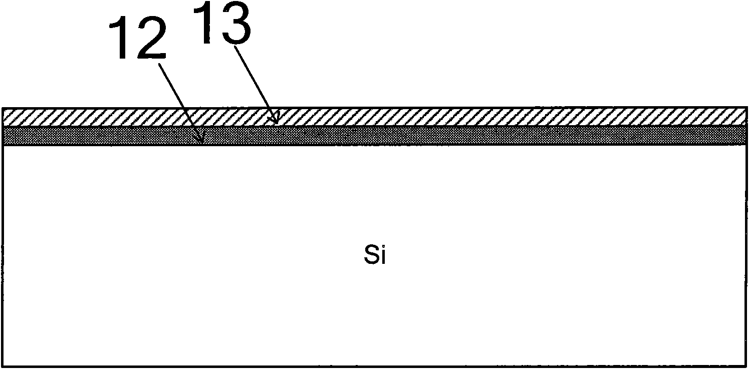
[0046] 1. If Figure 3-1 As shown, on the first surface of the high-resistance N-type silicon wafer as the substrate (ie Figure 3-1 Oxidation is carried out on the upper surface of the silicon drift detector, which is also the backside of the silicon drift detector finally made, to form a silicon dioxide layer 12 with a thickness of 1 μm; then chemical vapor deposition (LPCVD) with a thickness of for The silicon nitride layer 13;
[0047] 2. If Figure 3-2 As shown, photolithography is carried out on the surface of the silicon nitride layer 13, and the mask is etched, so as to obtain an expo...
PUM
 Abstract
Description
Claims
Application Information
 - R&D
- Intellectual Property
- Life Sciences
- Materials
- Tech Scout
- Unparalleled Data Quality
- Higher Quality Content
- 60% Fewer Hallucinations
Browse by: Latest US Patents, China's latest patents, Technical Efficacy Thesaurus, Application Domain, Technology Topic, Popular Technical Reports.
© 2025 PatSnap. All rights reserved.Legal|Privacy policy|Modern Slavery Act Transparency Statement|Sitemap|About US| Contact US: help@patsnap.com