1,550nm-waveband light beam tracking and communication integrated optical detection device

A technology of optical detection and space optical communication, applied in the field of space optical communication, can solve the problems of complex structure of space optical communication system, and achieve the effect of reducing the volume and simplifying the structure of the device

Active Publication Date: 2013-10-09
HARBIN INST OF TECH
View PDF3 Cites 0 Cited by
  • Summary
  • Abstract
  • Description
  • Claims
  • Application Information

AI Technical Summary

Problems solved by technology

[0003] The purpose of the present invention is to solve the problem of complex structure of the existing space optical communication system, and to provide an optical detection device integrating beam tracking and communication in the 1550nm band

Method used


Image

  • 1,550nm-waveband light beam tracking and communication integrated optical detection device
  • 1,550nm-waveband light beam tracking and communication integrated optical detection device
  • 1,550nm-waveband light beam tracking and communication integrated optical detection device

Examples


specific Embodiment approach 1

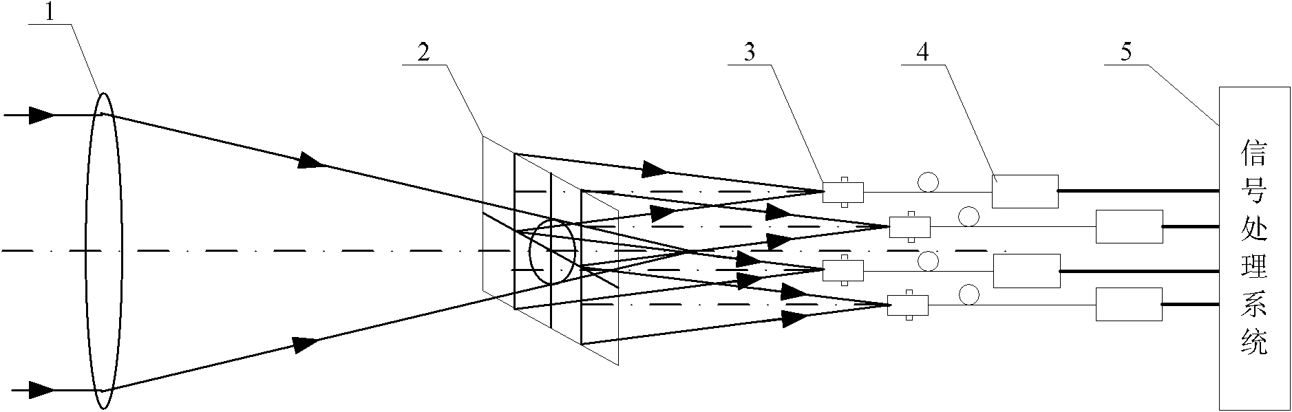
[0008] Specific implementation mode one: the following combination figure 1 This embodiment is described. This embodiment is composed of a main imaging lens 1, a 2×2 lens array 2, four optical fiber heads 3, four APD detectors 4 and a signal processing system 5.

[0009] The receiving light beam of the space optical communication system enters the main imaging lens 1, and after being focused by the main imaging lens 1, it enters the 2×2 lens array 2 and forms a spot on the 2×2 lens array 2. The spot formed on each lens Coupled into an optical fiber head 3, each optical fiber head 3 inputs its coupled optical signal to an APD detector 4, and each APD detector 4 converts the received optical signal into a voltage signal and outputs it to the signal processing system 5, the signal The processing system 5 processes the four voltage signals received at the same time to obtain the deflection angle of the optical axis of the received beam of the space optical communication system on ...

specific Embodiment approach 2

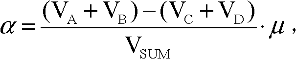
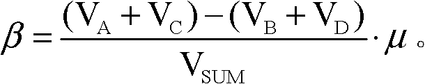
[0011] Specific implementation mode two: the following combination figure 1 Describe this embodiment, this embodiment is a further description of Embodiment 1, the method for the signal processing system 5 to process the voltage signal it receives is: set the four voltage signal values ​​received by the signal processing system 5 as V A , V B , V C and V D , where V A and V B The corresponding spot signal is on the two lenses in the same row of the 2×2 lens array 2, V C and V D The corresponding spot signal is on the two lenses in the other row of the 2×2 lens array 2, V A and V C The corresponding spot signal is on the two lenses in the same column of the 2×2 lens array 2, V B and V D The corresponding spot signal is on the two lenses of another column of the 2×2 lens array 2,

[0012] The communication processing part of the signal processing system 5 adds the four voltage signal values ​​to obtain the voltage and V SUM , its expression is: V SUM =V A +V B +V ...

specific Embodiment approach 3

[0019] Embodiment 3: This embodiment is a further description of Embodiment 2. The communication processing part of the signal processing system 5 converts the voltage and V SUM with the preset decision threshold V th are compared when V SUM >V th , carry out photoelectric decoding and output 1 code signal, when V SUM th , carry out photoelectric decoding and output a 0-code signal, and realize the communication with the receiving light beam of the space optical communication system.

[0020] In this embodiment, the optical signals of 0 and 1 codes input into the device are converted into 0 and 1 code point signals for photoelectric decoding to realize the communication function.

[0021] In the present invention, the 2×2 lens array 2 is located in front of the focal point of the main imaging lens 1 .

[0022] The main imaging lens 1 can be a transmissive telescope with an aperture of 80 mm and a focal length of 1 m.

[0023] The size of each lens in the 2×2 lens array 2 ...


PUM


Abstract

The invention discloses a 1,550-waveband light beam tracking and communication integrated optical detection device, which belongs to the technical field of space optical communication and solves the problem of complex structure of a conventional space optical communication system. A light beam received by the space optical communication system is incident into a main imaging lens, focused by the main imaging lens and incident to a 2*2 lens array, and forms light spots on the 2*2 lens array; the light spots formed on each lens are coupled into an optical fiber connector; each optical fiber connector inputs a light signal coupled per se into an avalanche photo diode (APD) detector; each APD detector converts the light signal received per se into a voltage signal, and outputs the voltage signal to a signal processing system; the signal processing system processes the four simultaneously received voltage signals to obtain deflection angles of the light beam received by the space optical communication system on a pitching axis and an azimuth axis; and the optical fiber lengths of the four optical fiber connectors are equal. The device is used for tracking the angle of light incidence of the space optical communication system.

Description

technical field [0001] The invention relates to an optical detection device integrated with 1550nm band beam tracking and communication, which belongs to the technical field of space optical communication. Background technique [0002] The space optical communication system uses light beams in the 1550nm band for communication, and it uses mature optical fiber devices to achieve high data rate information transmission. Due to the low sensitivity of the 1550nm band beam CCD detector and the large pixel size, the traditional space optical communication system uses the 1550nm band beam for signal transmission, and the 800nm ​​band laser is required as the beacon light at the transmitting end. It is necessary to use a CCD detector with a light beam in the 800nm ​​band to track the beacon light, which makes the overall structure of the system complex and consumes a lot of power. Contents of the invention [0003] The purpose of the present invention is to solve the problem of ...

Claims


Application Information

Patent Timeline
Patent Type & Authority Patents(China)
IPC IPC(8): H04B10/07G01B11/26G02B6/32H04B10/071H04B10/079
Inventor 韩琦琦于思源谭立英马晶俞建杰杨玉强赵生
Owner HARBIN INST OF TECH
Why Eureka
Try Eureka