New method for manufacturing interconnected copper pillars among plurality of layers of circuit boards

A technology of multi-layer circuit and new method, applied in the direction of multi-layer circuit manufacturing and the formation of electrical connection of printed components, etc., can solve the problems of circuit board stability and reliability effects, save plating time, stable and reliable performance, and practical sexual effect

Inactive Publication Date: 2011-07-06
王利平
View PDF0 Cites 10 Cited by
  • Summary
  • Abstract
  • Description
  • Claims
  • Application Information

AI Technical Summary

Problems solved by technology

This method leaves a nickel layer between the copper pillar and the copper layer, which affects the stability and reliability of the circuit board

Method used


Image

  • New method for manufacturing interconnected copper pillars among plurality of layers of circuit boards
  • New method for manufacturing interconnected copper pillars among plurality of layers of circuit boards
  • New method for manufacturing interconnected copper pillars among plurality of layers of circuit boards

Examples


Embodiment Construction

[0036] Below in conjunction with accompanying drawing and specific embodiment the present invention will be further described:

[0037] A new method for manufacturing interconnected copper pillars between layers of a multilayer circuit board, comprising the following steps:

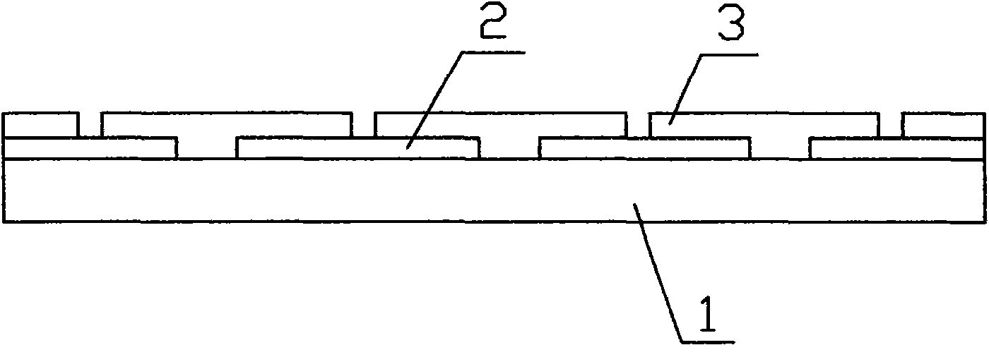
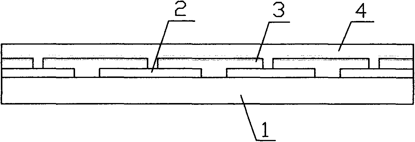
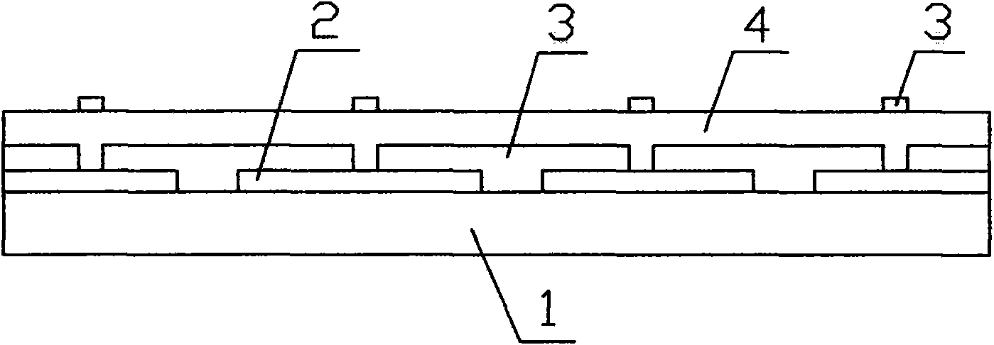
[0038] Step 1: If figure 1 As shown, a layer of permanent photosensitive layer 3 is coated or laminated on the copper foil 2 of the inner circuit board 1 , and the permanent photosensitive layer 3 is exposed to the position where the copper column needs to be electroplated after being exposed to light and developed.

[0039] Wherein the permanent photosensitive layer 3 can be dissolved or insoluble before the photosensitive reaction occurs, and after partial exposure, a local photosensitive reaction is triggered, and the part where the photosensitive reaction occurs cannot be dissolved or can be dissolved in water, alkaline water or an organic solvent. After the undissolved part of the permanent photosen...


PUM


Abstract

The invention relates to a new method for manufacturing interconnected copper pillars among a plurality of layers of circuit boards, comprising the following steps: 1, coating or laminating a permanent photosensitive layer on the inner-layer circuit boards, and exposing the parts needing to be electroplated with the copper pillars after light sensitivity and developing; 2, through chemically plating copper, leading copper layers to reach the height needed by the copper pillars; 3, coating or laminating a temporary light-sensitive layer, and remaining the light-sensitive layer for protecting the light-sensitive layer of the copper pillars after light sensing and developing; 4, obtaining the copper pillars for interconnection needing among the layers by etching; 5, removing the temporary light-sensitive layer; 6, obtaining new copper layers by chemically plating copper plating and electroplating copper for thickening after surface treatment; and 7, manufacturing an outer-layer circuit on the new copper layers. Compared with the prior art, in the new method, large-area and large-current copper plating is adopted so as to omit electroplating a nickel layer, save the electroplating time and improve the efficiency; and the connection among the copper pillars and copper layers is firm, so that the performance of the plurality of layers of the circuit boards is more stable and reliable and the circuit boards have practicability.

Description

technical field [0001] The invention relates to a circuit board manufacturing process, in particular to a new method for manufacturing interconnected copper pillars between layers of a multilayer circuit board. Background technique [0002] The existing high-density multi-layer printed circuit board made of copper pillar method to achieve interlayer interconnection does not need to drill holes on the circuit board, thus eliminating the need for expensive laser drilling machines, and has high reliability and low manufacturing cost. Etc. At present, there are two main methods of manufacturing copper pillars between layers of multilayer circuit boards: [0003] The first method consists of the following five steps: [0004] 1. First, coat or press a photosensitive resin layer on the surface of the circuit board with the inner layer circuit, and develop the electroplated copper column by photosensitive development; [0005] 2. Electroplating to form copper pillars; [0006] ...

Claims


Application Information

Patent Timeline
Patent Type & Authority Applications(China)
IPC IPC(8): H05K3/40H05K3/46
Inventor 王利平
Owner 王利平
Why Eureka
Try Eureka