Memory cell suitable for dram memory

A memory cell and memory technology, applied in the direction of capacitors, electrical components, electric solid devices, etc., can solve the problems of increased danger of junction leakage, problematic process temperature, negative memory effect, etc., to reduce the danger of junction leakage, manufacturing Low cost and reduced temperature problems

Inactive Publication Date: 2011-07-13
NXP BV
View PDF4 Cites 4 Cited by
  • Summary
  • Abstract
  • Description
  • Claims
  • Application Information

AI Technical Summary

Problems solved by technology

[0003] The disadvantage of adopting trench capacitors with high aspect ratio in sub-100nm technology is low yield
Another disadvantage is increased manufacturing costs
Also, the use of new low-k materials for dielectric layers is problematic in terms of the process temperatures used in typical CMOS processes
Also, the scaling of trench capacitors and stack capacitors suffers from an increased risk of junction leakage, which has a negative effect on the memory effect
[0004] Another technical issue with scaling DRAM memory cells involves the cell transistors

Method used


Image

  • Memory cell suitable for dram memory
  • Memory cell suitable for dram memory
  • Memory cell suitable for dram memory

Examples


Embodiment Construction

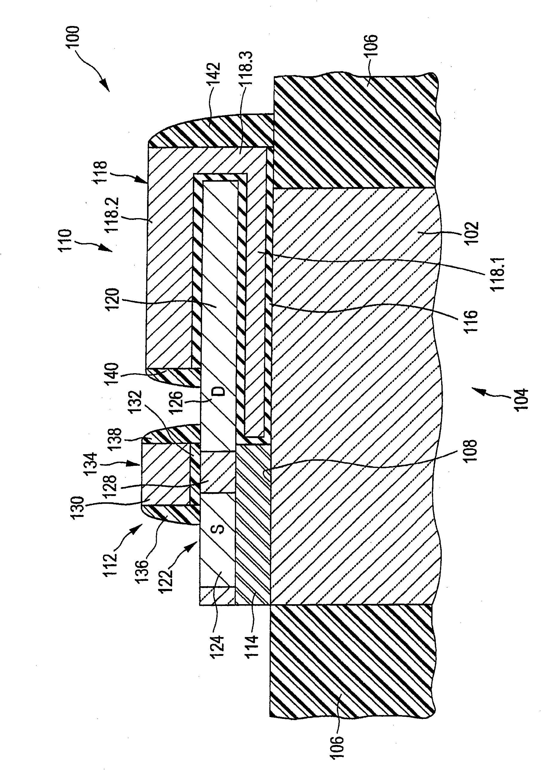
[0061] figure 1 A schematic cross-sectional view of a memory cell 100 according to a first embodiment of the invention is shown. The memory cell 100 is disposed on a silicon substrate 102 . On a silicon substrate, an active semiconductor region 104 is laterally bounded by shallow trench isolation (STI) regions 106, as is well known in CMOS technology. figure 1 Only a portion of substrate 102 is shown. The portion includes an active semiconductor region having a substantially planar surface 108 . The substrate 102 is only shown to a depth that does not exceed the depth of the shallow trench isolation regions. Notice, figure 1 The illustration of the memory cells in is purely schematic and is not intended to fully reflect geometrical proportions.

[0062] On the active semiconductor region 104, active elements of the memory cell 100 are arranged. That is, the memory capacitor 110 and the control MOSFET 112 are provided on the active semiconductor region. Note that the sur...


PUM


Abstract

The present invention relates to a memory cell with a memory capacitor (110) on an active semiconductor region (104), the memory capacitor having a first capacitor- electrode layer, which, in a cross-sectional view of the memory cell, has first and second electrode-layer sections that extend on the active semiconductor region in parallel to the surface of the active semiconductor region at a vertical distance to each other and that are electrically connected by a third electrode-layer section extending vertically, that is, perpendicular to the surface of the active semiconductor region. A control transistor (112) is connected with a conductive second capacitor electrode layer that extends between the first and second electrode-layer sections and is electrically isolated from them by an isolation layer (116). Achieved advantages comprise a high manufacturing yield can, reduced fabrication cost and reduced risk of junction leakage by a small area required for the memory cell.

Description

technical field [0001] The present invention relates to memory cells and memory devices. Background technique [0002] W. Mueller et al. review the concept of scaling DRAM memory cells to 40nm in "Challenges for the DRAM Cell Scaling to 40nm", IEDM Tech. Dig., 2005, pp. 336-339. The technical issues discussed for DRAM capacitors focus on trench capacitors on the one hand and stack capacitors on the other. Scaling trench capacitors with constant cell capacitance is described as requiring increasing aspect ratios up to 120 and / or using alternative high-k dielectric materials. Similar requirements have also been reported for stacked capacitors. [0003] The disadvantage of employing trench capacitors with high aspect ratios in sub-100nm technologies is low yield. Another disadvantage is increased manufacturing costs. Also, the use of new low-k materials for dielectric layers is problematic in terms of process temperatures used in typical CMOS processes. Also, the scaling o...

Claims


Application Information

Patent Timeline
Patent Type & Authority Applications(China)
IPC IPC(8): H01L21/8242H01L27/07H01L21/02H01L27/108H01L27/02
CPCH01L27/1082H01L28/87H01L27/0733H01L27/0207H01L27/1085H10B12/33H10B12/03
Inventor 苏菲·普吉特帕思卡儿·L·A·马佐耶
Owner NXP BV
Why Eureka
Try Eureka