Device and method for enhancing atomic layer deposition by pulse-modulation radio frequency plasma
A technology of radio frequency plasma and atomic layer deposition, which is applied in the field of plasma assistance, can solve problems affecting the quality of deposited films and limit the use of temperature-sensitive substrate materials, so as to ensure the quality of deposited films and prevent the rise and decrease of chamber temperature. effect of influence
- Summary
- Abstract
- Description
- Claims
- Application Information
AI Technical Summary
Problems solved by technology
Method used
Image
Examples
Embodiment 1
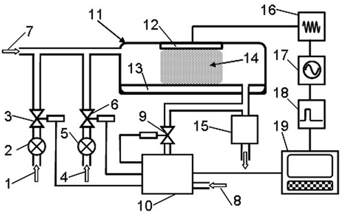
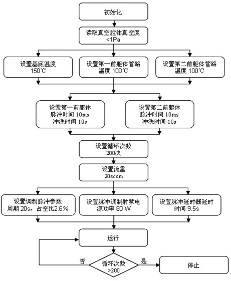
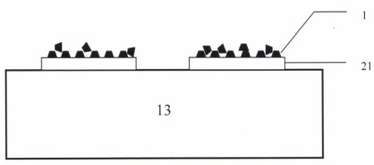
[0026] Such as figure 1As shown, it is a schematic structural diagram of a pulse-modulated radio-frequency plasma-enhanced atomic layer deposition device. The pulse-modulated radio-frequency plasma-enhanced atomic layer deposition device includes a first precursor manual valve 2, a first precursor pneumatic valve 3, a second precursor Body manual valve 5, second precursor pneumatic valve 6, brake gas pneumatic valve 9, integrated control module 10, vacuum reaction chamber 11, plasma electrode 12, substrate 13 (as a ground electrode), vacuum mechanical pump 15, radio frequency Power matching device 16, pulse modulation radio frequency power supply 17, pulse delayer 18 and computer 19. The bottom of the vacuum reaction chamber 11 is provided with a substrate 13, the vacuum reaction chamber 11 is respectively connected to the vacuum mechanical pump 15 and the precursor input pipeline, the top of the vacuum reaction chamber 11 is provided with a plasma electrode 12, and the plasma...
Embodiment 2
[0040] Similar to Embodiment 1, the difference is that quartz glass is used as the material of the substrate 21, and the plasma electrode 12 is an aluminum electrode with a thickness of 10 mm. The height of the vacuum reaction chamber 11 is 50 mm. The substrate temperature is set to 200°C, the power of the RF power matcher 16 is adjusted to 100W, and other parameter settings and processes are consistent with those in Example 1, and uniformly deposited Al can also be obtained on the quartz glass substrate. 2 o 3 film.
Embodiment 3
[0042] Similar to Example 1, the difference is that polyethylene terephthalate is used as the material of the substrate 21, and the plasma electrode 12 is a copper electrode with a thickness of 5 mm. The height of the vacuum reaction chamber 11 is 40 mm. Set the substrate temperature to 60°C, adjust the power of the RF power matcher 16 to 70W, and other parameter settings and processes are consistent with those in Example 1, and uniformly deposited Al can also be obtained on the PET substrate. 2 o 3 film.
PUM
| Property | Measurement | Unit |
|---|---|---|
| Thickness | aaaaa | aaaaa |
| Height | aaaaa | aaaaa |
| Thickness | aaaaa | aaaaa |
Abstract
Description
Claims
Application Information


