Wafer-level low-temperature packaging method based on gold-tin alloy bonding

An encapsulation method and tin alloy technology, which are applied in the process of producing decorative surface effects, decorative arts, microstructure devices, etc., can solve the problems of high cost, complex process, incompatibility, etc., and achieve reliable industrialization and commercialization , The process is simple to implement, and the effect of reducing the total thickness

Active Publication Date: 2011-07-20
INST OF SEMICONDUCTORS - CHINESE ACAD OF SCI
View PDF1 Cites 19 Cited by
  • Summary
  • Abstract
  • Description
  • Claims
  • Application Information

AI Technical Summary

Problems solved by technology

[0019] At present, Au-Sn alloy bonding consumes more precious metal Au, the cost is higher, the bonding layer is thicker and the bonding temperature is still relatively high for MEMS devices (especially microfluidic devices, BioMEMS devices, etc.) and integrated circuits. higher
Wafer-level low-temperature packaging methods are roughly divided into the following three categories: The first is polymer or adhesive layer bonding. In this method, the thermal conductivity of the polymer or adhesive layer is generally poor, and water vapor and gas can easily pass through the bond. Therefore, it is not possible to achieve a good airtight package, it is not compatible with vacuum packaging, and the reliability of bonding is poor
The second is to choose an alloy bonding material with a lower bonding temperature. For example, Sn-In alloy bonding can be completed at 118 ° C, but it belongs to a "soft" solder, and its bonding strength, air tightness and reliability Both are worse than Au-Sn alloy
The third method is local heating bonding, such as local resistance heating, induction heating, electromagnetic radiation heating, laser-assisted heating and other local heating bonding methods, but these processes have the characteristics of expensive equipment, complicated process and difficult operation.
[0020] In short, the above-mentioned low-temperature methods have different restrictions on the wafer-level packaging of MEMS devices, and cannot fully meet the requirements. There is an urgent need to develop simpler and more effective low-cost low-temperature packaging methods.

Method used


Image

  • Wafer-level low-temperature packaging method based on gold-tin alloy bonding
  • Wafer-level low-temperature packaging method based on gold-tin alloy bonding
  • Wafer-level low-temperature packaging method based on gold-tin alloy bonding

Examples


Embodiment Construction

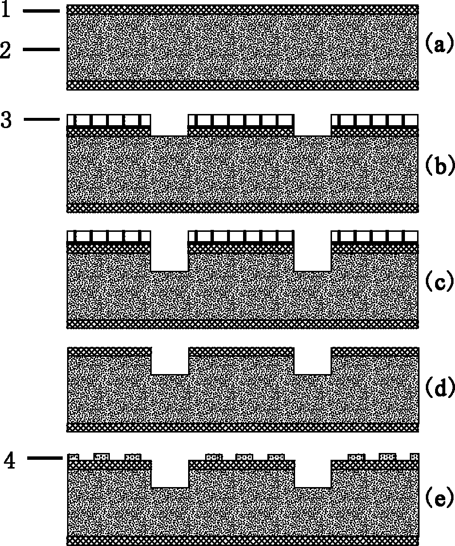
[0047] In order to make the object, technical solution and advantages of the present invention clearer, the present invention will be further described in detail below by taking the bonding of Si cover sheet and Si back sheet as an example and referring to the accompanying drawings.

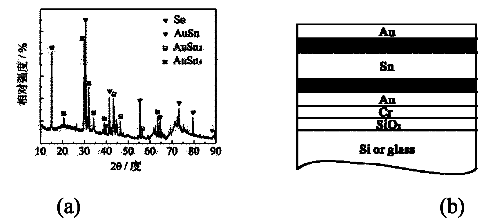
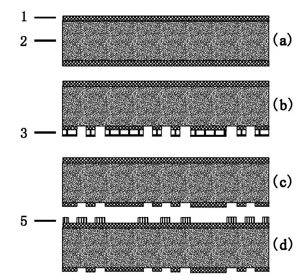
[0048] The invention provides a wafer-level low-temperature packaging method based on Au-Sn alloy bonding. The method includes: selecting a substrate as a cover sheet and a bottom sheet; performing photolithography on the front of the cover sheet for the first time, through etching and Etching creates a cavity as a placement space for the packaged device or structure; performs a second photolithography on the front of the cover sheet; evaporates a multilayer metal film of Cr / Au / Sn / Au according to the designed weight percentage of Au and Sn; Peel off the multi-layer metal film to make the metal bonding structure on the cover sheet; carry out the first photolithography on the back of the negative, e...


PUM

PropertyMeasurementUnit
thicknessaaaaaaaaaa
thicknessaaaaaaaaaa
shear strengthaaaaaaaaaa

Abstract

The invention discloses a wafer-level low-temperature packaging method based on gold-tin alloy bonding, a tin-rich (Sn) alloy component is selected, Sn content is equal to 54%-71%, the gold thickness and the tin thickness are designed to be less than 2.1 mu m and 0.7 mu m respectively, and the gold-tin alloy bonding is performed at a certain pressure and a certain temperature within certain time, thereby forming an intermediate layer which is based on an AuSn2 phase (that is an epsilon phase) with high Vickers hardness and realizing the wafer-level low-temperature packaging method with low cost and high bonding strength. The bonding temperature is 140-310 DEG C, and the bonding strength as high as 20-64MPa can be realized. The wafer-level low-temperature packaging method which has the advantages of low cost and high bonding strength can be applied in packaging of devices on any substrates.

Description

technical field [0001] The invention relates to a packaging method in the fields of MEMS devices, photoelectric devices, microelectronic devices and integrated circuits, and provides a low-cost, high-bonding strength wafer-level low-temperature packaging method based on gold-tin (Au-Sn) alloy bonding. Background technique [0002] Micro-Electro-Mechanical Systems (MEMS) is the product of the integration of microelectronics and micromechanics. It combines the silicon microfabrication technology in the integrated circuit manufacturing process and the micromachining technology in the machinery industry to create an optical, mechanical and electrical integration. of new devices. After more than ten years of development, MEMS chips have been quite mature, but many chips have not been practically used as products. One of the main reasons is the packaging problem. [0003] Wafer-level packaging is more attractive in MEMS packaging due to its advantages of low cost, high yield, sma...

Claims


Application Information

Patent Timeline
Patent Type & Authority Applications(China)
IPC IPC(8): H01L21/60H01L21/50B81C1/00
Inventor 毛旭杨晋玲杨富华
Owner INST OF SEMICONDUCTORS - CHINESE ACAD OF SCI
Why Eureka
Try Eureka