Laterally diffused MOSFET (LDMOS) and method for manufacturing same

A manufacturing method and technology of injection area, which are applied in semiconductor/solid-state device manufacturing, electrical components, circuits, etc., can solve the problems of increasing device area, achieve good balance and improve the effect of breakdown voltage

Active Publication Date: 2012-11-07
SHANGHAI HUAHONG GRACE SEMICON MFG CORP
View PDF0 Cites 0 Cited by
  • Summary
  • Abstract
  • Description
  • Claims
  • Application Information

AI Technical Summary

Problems solved by technology

These changes either have a relatively large impact on the device's on-resistance Rdson, saturation current and other parameters, or will cause the area of ​​the device to increase

Method used


Image

  • Laterally diffused MOSFET (LDMOS) and method for manufacturing same
  • Laterally diffused MOSFET (LDMOS) and method for manufacturing same
  • Laterally diffused MOSFET (LDMOS) and method for manufacturing same

Examples


Embodiment Construction

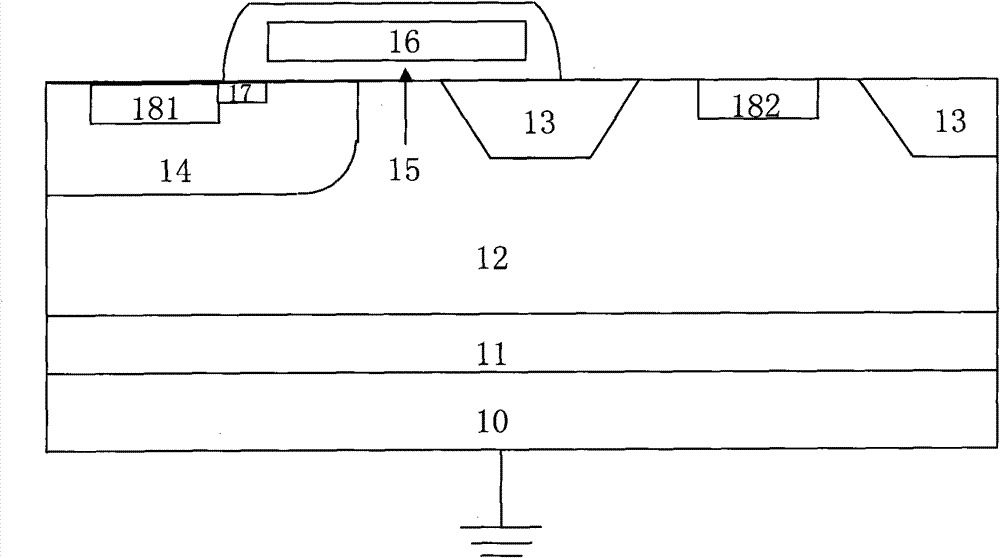
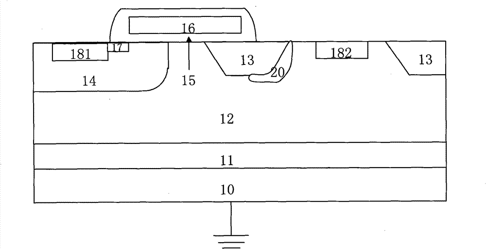
[0020] see figure 2 , the LDMOS device of the present invention has a p-type epitaxial layer 11 and an n well 12 on a p-type silicon substrate 10 . Since the n-well 12 is relatively deep, it is also commonly referred to as a deep n-well 12 . In the n-well 12 there is an isolation structure 13 and a low-voltage p-well 14 . Above the n-well 12 is a gate oxide layer 15 and a gate 16, and the gate 16 is surrounded by a dielectric to form a floating gate. One end of the gate 16 is above the low-voltage p-well 14 , and the other end is above the isolation structure 13 . The low-voltage p-well 14 has an n-type lightly doped drain implantation region 17 and an n-type heavily doped drain implantation region 181, and the n-type heavily doped drain implantation region 181 serves as the source of the LDMOS device. The n-well 12 also has an n-type heavily doped drain implant region 182, serving as the drain of the LDMOS device.

[0021] Compared with the traditional LDMOS device, the ...


PUM


Abstract

The invention discloses a laterally diffused MOSFET (LDMOS). Compared with the conventional MDMOS, the laterally diffused MOSFET is characterized in that: a p-type ion implantation zone (20) is added at the bottom and / or side wall of one side, close to the drain (182) in the n-well (12), of the isolation structure (13) between the source (181) and the drain (182). By adoption of the added p-type ion implantation zone (20), the appearances of the electric charge distribution and the depletion region are changed, the breakdown voltage (BV) of LDMOS device is improved, the Rdson of LDMOS device is basically free from influence and a better balance between BV and Rdson is realized.

Description

technical field [0001] The invention relates to a semiconductor integrated circuit device, in particular to an LDMOS (laterally diffused MOSFET, laterally diffused MOS transistor) device. Background technique [0002] see figure 1 , which is a schematic cross-sectional view of a conventional LDMOS device. A p-type epitaxial layer 11 and an n-well 12 are provided on a p-type silicon substrate 10 . Since the n-well 12 is relatively deep, it is also commonly referred to as a deep n-well 12 . In the n-well 12 there is an isolation structure 13 and a low-voltage p-well 14 . Above the n-well 12 is a gate oxide layer 15 and a gate 16, and the gate 16 is surrounded by a dielectric to form a floating gate. One end of the gate 16 is above the low-voltage p-well 14 , and the other end is above the isolation structure 13 . The low-voltage p-well 14 has an n-type lightly doped drain implantation region 17 and an n-type heavily doped drain implantation region 181, and the n-type heav...

Claims


Application Information

Patent Timeline
Patent Type & Authority Patents(China)
IPC IPC(8): H01L29/78H01L29/06H01L21/336H01L21/265
CPCH01L29/7816H01L29/0619H01L29/0653
Inventor 张帅戚丽娜胡君
Owner SHANGHAI HUAHONG GRACE SEMICON MFG CORP
Why Eureka
Try Eureka