Novel integrated circuit structure of full-integrated dual frequency band low-noise amplifier

A low-noise amplifier and integrated circuit technology, applied in the direction of improving the amplifier to expand the bandwidth, etc., can solve the problem that the broadband transmission system cannot be used

Inactive Publication Date: 2015-04-08
SOUTHEAST UNIV +1
View PDF3 Cites 0 Cited by
  • Summary
  • Abstract
  • Description
  • Claims
  • Application Information

AI Technical Summary

Problems solved by technology

The disadvantage is that it can only be used in narrowband applications and cannot be used in broadband transmission systems

Method used


Image

  • Novel integrated circuit structure of full-integrated dual frequency band low-noise amplifier
  • Novel integrated circuit structure of full-integrated dual frequency band low-noise amplifier
  • Novel integrated circuit structure of full-integrated dual frequency band low-noise amplifier

Examples


Embodiment Construction

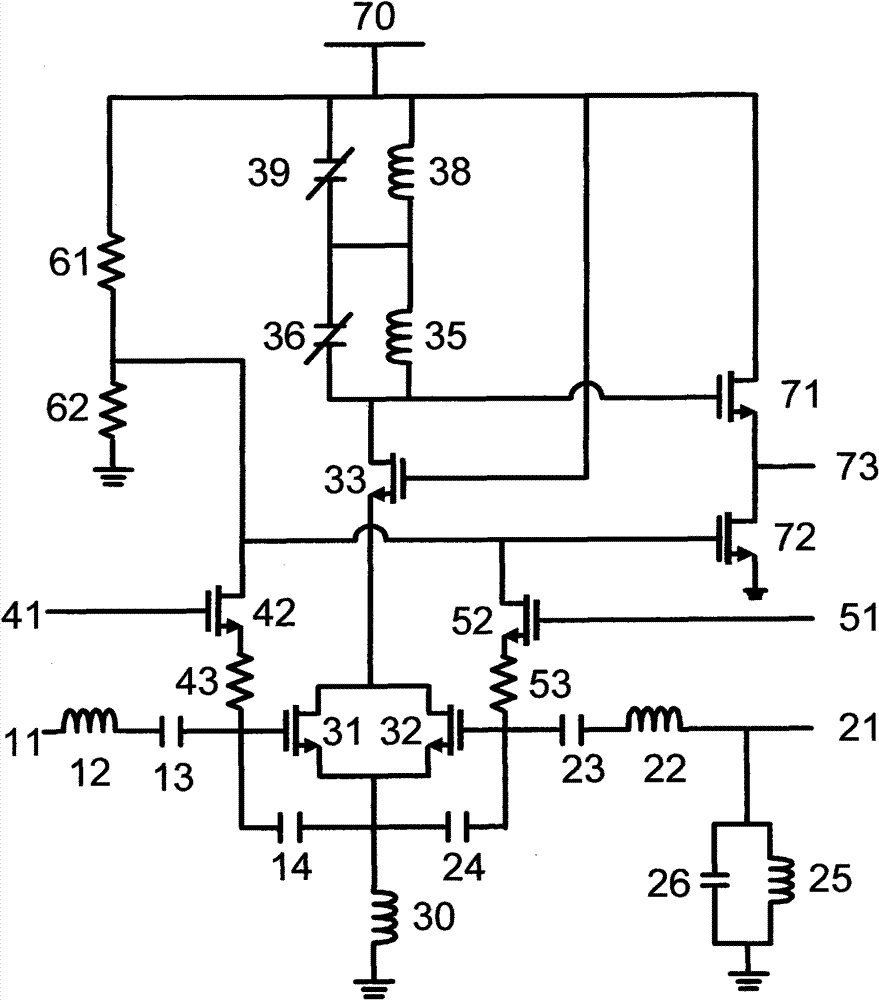
[0083] exist figure 1 In , the circuit topology diagram can be divided into the following five parts:

[0084] The first part consists of the inductor L S , L 1 , L 2 , L 3 and capacitance C 1 , C 2 , C 3 , C ext1 , C ext2 . Inductance L 2 , L 3 and capacitance C 2 , C 3 Form a band-pass filter for widening the frequency band; inductance L 1 and capacitance C 1 and inductance L S , for input impedance matching; capacitor C ext1 , C ext2 Connect across the gate-source terminals of the two amplifier transistors for optimal noise matching.

[0085] The second part consists of NMOS transistors M 1 ,M 2 ,M 3 , inductance L L1 , L L2 and capacitance C L1 , C L2 . NMOS transistor M 1 ,M 2 Is the amplifier tube, NMOS transistor M 3 respectively with M 1 ,M 2 Form a cascode structure; inductance L L1 , L L2 with capacitance C L1 , C L2 form two parallel resonant networks, capacitor C L1 , C L2 It is two variable capacitors, whose capacitance value i...


PUM


Abstract

The invention provides an integrated circuit structure of a dual frequency band low-noise amplifier, which can be applied to a multi-frequency-band multi-standard communication system of advanced international mobile communication (IMT-Advanced) and ultra-wide band (UWB) communication, and relates to the field of integrated circuits. Compared with the disclosed structures, the integrated circuit structure provided by the invention has the advantages that: the input end of the integrated circuit structure adopts a narrow band input matching network and a broad band input matching network in two frequency bands so as to realize 50-ohm impedance matching within the frequency bands of (3.4-3.6GHz and 4.2-4.8GHz) in different bandwidths; two parallel resonance networks are used as a load; an external control signal is used for controlling a resonance frequency so as to meet different gain requirements of two frequency bands, expand the bandwidth of the circuit, enhance the gain flatness of the circuit on the whole working bandwidth and ensure that a digital signal controls switching of the frequency bands. Compared with the prior art, the integrated circuit structure provided by the invention is characterized by great improvement on the noise coefficient, the gain and a matching technology index of input and output. The design of the integrated circuit structure is tested by using a 0.13-millimeter mixed signal complementary metal-oxide-semiconductor process of SMIC Company, and the result proves the feasibility of the structure.

Description

technical field [0001] The invention relates to a fully-integrated dual-band low-noise amplifier integrated circuit chip, especially a multi-channel chip that can be simultaneously applied to advanced international mobile communications (Advanced International Mobile Communications, IMT-Advanced) and ultra-wideband (Ultra-Wide Band, UWB) communications. A dual-band low-noise amplifier integrated circuit chip for multi-band, multi-standard communication systems. Background technique [0002] At present, an important trend in the development of mobile communication is that a single communication terminal can be compatible with multiple communication standards (Agnelli F., Albasini G., Bietti I., Gnudi A., et al, "Wirelessmulti-standard terminals system analysis and design of a reconfigurableRF front-end", Circuits and Systems Magazine, IEEE Volume 6, Issue 1, First Quarter 2006 Page(s): 38-59, reference 1), such as the third generation (3G) cellular mobile communication system...

Claims


Application Information

Patent Timeline
Patent Type & Authority Patents(China)
IPC IPC(8): H03F1/42
Inventor 黄风义王燕唐旭升姜楠
Owner SOUTHEAST UNIV
Why Eureka
Try Eureka