

Bipolar semiconductor device and method for manufacturing same
A semiconductor and bipolar technology, applied in semiconductor/solid-state device manufacturing, semiconductor devices, semiconductor/solid-state device components, etc., can solve problems such as difficulty in reducing density and improving the performance of bipolar transistors, and achieve increased current increase The effect of high efficiency, low cost and simple process
- Summary
- Abstract
- Description
- Claims
- Application Information
AI Technical Summary
Problems solved by technology
Method used
Image

Examples
Embodiment approach 1
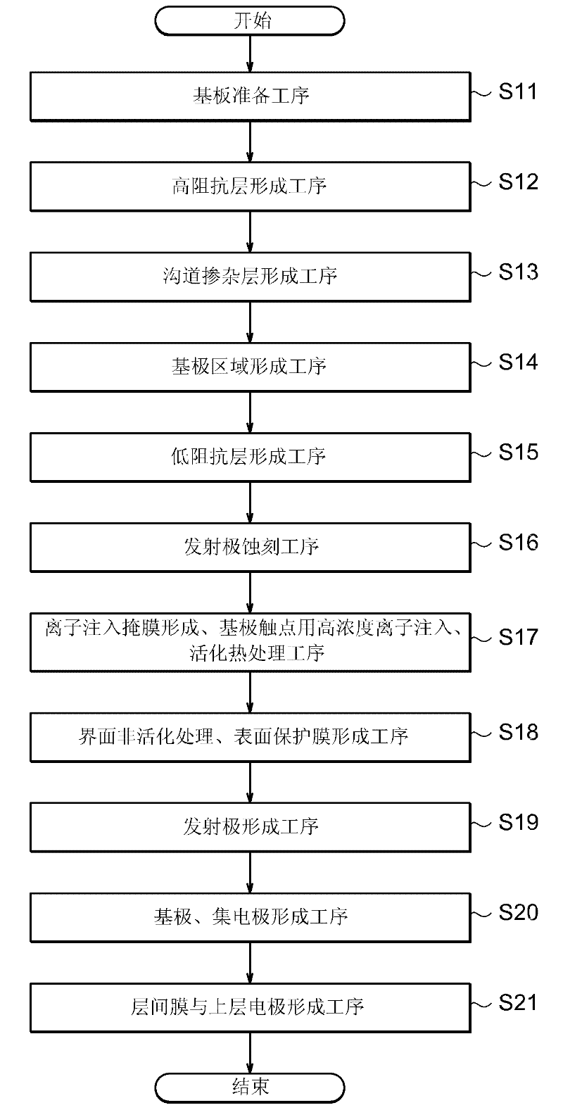
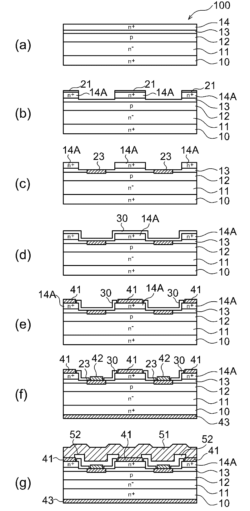
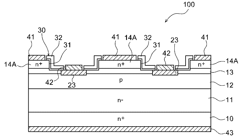
[0041] Refer below Figure 1 ~ Figure 3 , Embodiment 1 of the bipolar semiconductor device of the present invention will be described. The bipolar semiconductor device is an example of a BJT. refer to Figure 1 ~ Figure 3 The manufacturing method and structure of the BJT will be described. figure 1 It is a flowchart showing each step of the manufacturing method. figure 2 (a) to (g) show the cross section of BJT100 produced in each process. image 3 will be figure 2 (f) in (f) is enlarged and shows the detailed structure of the surface protection film.
[0042] The manufacturing method of BJT is comprised by the following flow|flow (1)-(11) (step S11-S21). like figure 1 As shown, each process is executed in the order of step S11 to step 21. (1) Substrate (crystal) preparation process of n+ type low-resistance SiC semiconductor element (step S11)
[0043] (2) Formation process of n-type high impedance conductor (step S12)
[0044] (3) Step of forming a p-type chann...
Embodiment approach 2
[0082] Refer below Figure 4 , the second embodiment of the bipolar semiconductor device of the present invention will be described. The bipolar semiconductor device in Embodiment 2 is BJT200. Compared with the first embodiment, the BJT200 manufacturing process of the second embodiment differs only in the content of the interface deactivation treatment and the surface protection film formation process (step S18), and the other processes (steps S11-S17, S19-S21) are different from those of the first embodiment. A BJT manufacturing process is the same.
[0083] Figure 4 Shown is a cross-sectional structural diagram in a state where the emitter 41 , the base 42 , and the collector 43 have already been formed. In the second embodiment, steps S18 "(1) Inactivation treatment of the SiC surface" and "(2) Formation and heat treatment of the surface protection film" are the same as those in the first embodiment. In step S18 of Embodiment 2, the SiNx deposition process is carried o...
Embodiment approach 3
[0089] Refer below Figure 5 , Embodiment 3 of the bipolar semiconductor device of the present invention will be described. The bipolar semiconductor device of Embodiment 3 is a pn diode 300 . and figure 2 Compared with the multilayer structure shown in (a), the multilayer structure when the semiconductor device is a pn diode 300 is composed of a two-layer structure composed of the negative electrode region 61 and the positive electrode region 62 . In the pn diode 300, the exposed SiC surface is similarly subjected to an interface deactivation treatment and a surface protective film forming process. The content of this step is the same as that of step S18 described in the first embodiment. Other manufacturing steps are determined or changed according to the manufacturing steps of pn diodes. A negative electrode 63 is formed in the negative electrode region 61 , and a positive electrode 64 is formed in the positive electrode region 62 . In addition, as in Embodiment 1, on...
PUM
| Property | Measurement | Unit |
|---|---|---|
| Film thickness | aaaaa | aaaaa |
| Thickness | aaaaa | aaaaa |
| Film thickness | aaaaa | aaaaa |
Abstract
Description
Claims
Application Information