Supercharge Your Innovation With Domain-Expert AI Agents!

Method for manufacturing CMOS image sensor

A technology of an image sensor and a manufacturing method, which is applied in the field of semiconductors, and can solve problems such as substrate etching in the CMOS transistor area, increased leakage current of the MOS transistor, and failure of the MOS transistor to work normally, so as to reduce damage and avoid repeated etching Effect

Inactive Publication Date: 2011-07-27
SEMICON MFG INT (SHANGHAI) CORP +1
View PDF1 Cites 3 Cited by
  • Summary
  • Abstract
  • Description
  • Claims
  • Application Information

AI Technical Summary

Problems solved by technology

[0008] However, during the etching process of the spacer, the problem that the substrate of the CMOS transistor region is etched often occurs, and the substrate damage of the CMOS transistor region will increase the leakage current of the MOS transistor, so that the MOS transistor cannot Normal work, CMOS image sensor performance degradation

Method used


Image

  • Method for manufacturing CMOS image sensor
  • Method for manufacturing CMOS image sensor
  • Method for manufacturing CMOS image sensor

Examples


Embodiment Construction

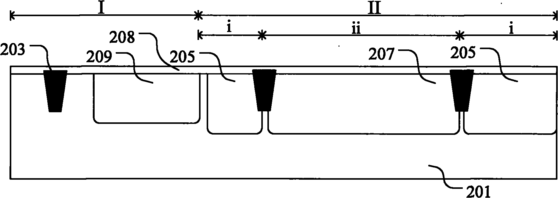
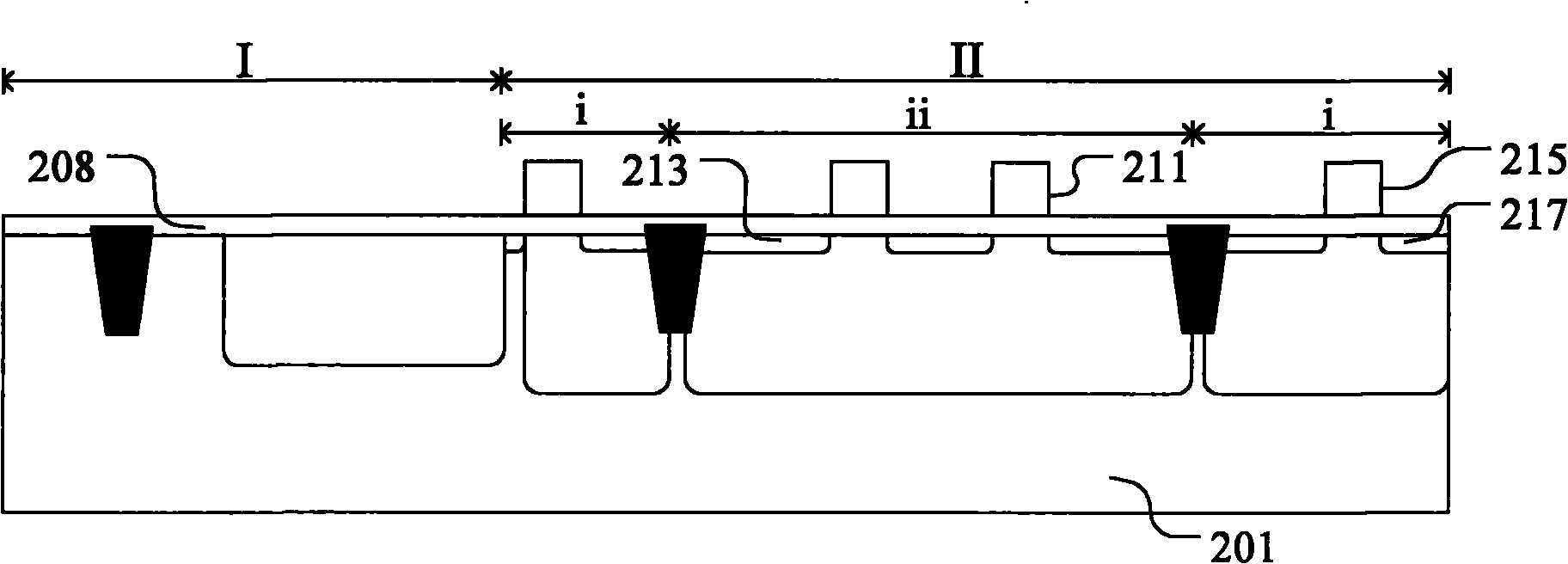
[0029] In the prior art, when manufacturing a CMOS image sensor, it is necessary to form a substrate protection layer on the semiconductor substrate in the photodiode region to protect the surface of the semiconductor substrate. The substrate protection layer is usually formed simultaneously with the spacers of the CMOS transistors, which requires two photolithography and etching processes, that is, the spacers of the PMOS transistors and the spacers of the NMOS transistors are formed respectively.

[0030] In the process of forming the MOS transistor spacer, if there is a deviation in the photolithographic alignment or an error in the subsequent photoresist development, the photoresist mask will have a pattern deviation, and the pattern deviation of the photoresist mask will make the semiconductor substrate The bottom is etched repeatedly, causing damage to the substrate. The damage of the semiconductor substrate will increase the leakage current of the MOS transistor, so tha...


PUM


Abstract

The invention relates to a method for manufacturing a complementary metal oxide semiconductor (CMOS) image sensor. The CMOS image sensor comprises a CMOS transistor. A method for forming the gap wall of the CMOS transistor comprises the following steps of: forming a gap wall dielectric layer on a semiconductor substrate and a gate electrode, and forming a photoresist layer on the gap wall dielectric layer; imaging the photoresist layer, and retaining a photodiode area and the photoresist layer on the gap wall dielectric layer in a light doping area on one side, which is adjacent to the photodiode area, of a metal oxide semiconductor (MOS) transistor adjacent to the photodiode area; and etching the gap wall dielectric layer by taking the photoresist layer as a mask to form the gap wall of the MOS transistor, wherein the MOS transistor adjacent to the photodiode area forms the gap wall only on one side of the gate electrode which is away from the photodiode area, and the gap wall dielectric layer retained in the photodiode area is used as a substrate protective layer of the semiconductor substrate in the photodiode area simultaneously.

Description

technical field [0001] The present invention relates to the technical field of semiconductors, and more specifically, the present invention relates to a method for manufacturing a CMOS image sensor. Background technique [0002] An image sensor is a semiconductor device that converts light signals into electrical signals. Image sensors are generally classified into two categories: Charge Coupled Devices (Charger Coupled Device, CCD) and Complementary Metal Oxide Semiconductor (CMOS) image sensors. CCD image sensor has the advantages of low read noise, large dynamic range, and high response sensitivity. However, CCD image sensor has high power consumption and complicated manufacturing process, making it difficult to realize single-chip integration with peripheral circuits. [0003] The CMOS image sensor adopts the same CMOS technology as the signal processing circuit, and the CMOS image sensor and the signal processing circuit outside the sensor can be integrated on the same...

Claims


Application Information

Patent Timeline
Patent Type & Authority Applications(China)
IPC IPC(8): H01L27/146
CPCH01L27/14689H01L27/14612
Inventor 霍介光杨建平
Owner SEMICON MFG INT (SHANGHAI) CORP
Features
  • R&D
  • Intellectual Property
  • Life Sciences
  • Materials
  • Tech Scout
  • Unparalleled Data Quality
  • Higher Quality Content
  • 60% Fewer Hallucinations
Learn More