Nanometer-level automatic focusing system for projection lithography

An automatic focusing and projecting light technology, which is applied in microlithography exposure equipment, optics, photography, etc., can solve the problems of lower measurement efficiency, low degree of automation, and increased calculation amount, and achieve simple operation and automation High, high production efficiency effect

Inactive Publication Date: 2011-08-03
INST OF OPTICS & ELECTRONICS - CHINESE ACAD OF SCI
View PDF3 Cites 20 Cited by
  • Summary
  • Abstract
  • Description
  • Claims
  • Application Information

AI Technical Summary

Problems solved by technology

This method can achieve a certain accuracy, but with the increase of the number of subdivisions, the calculation amount will increase and the measurement efficiency will be reduced.
The focusing method based on the diffraction grating mark reflects the defocus amount of the silico

Method used


Image

  • Nanometer-level automatic focusing system for projection lithography
  • Nanometer-level automatic focusing system for projection lithography
  • Nanometer-level automatic focusing system for projection lithography

Examples


Embodiment Construction

[0027] In order to make the object, technical solution and advantages of the present invention clearer, the present invention will be described in further detail below in conjunction with specific embodiments and with reference to the accompanying drawings.

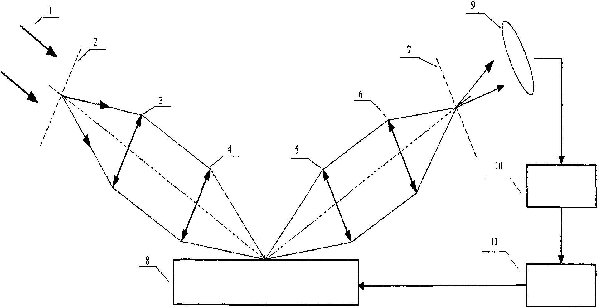
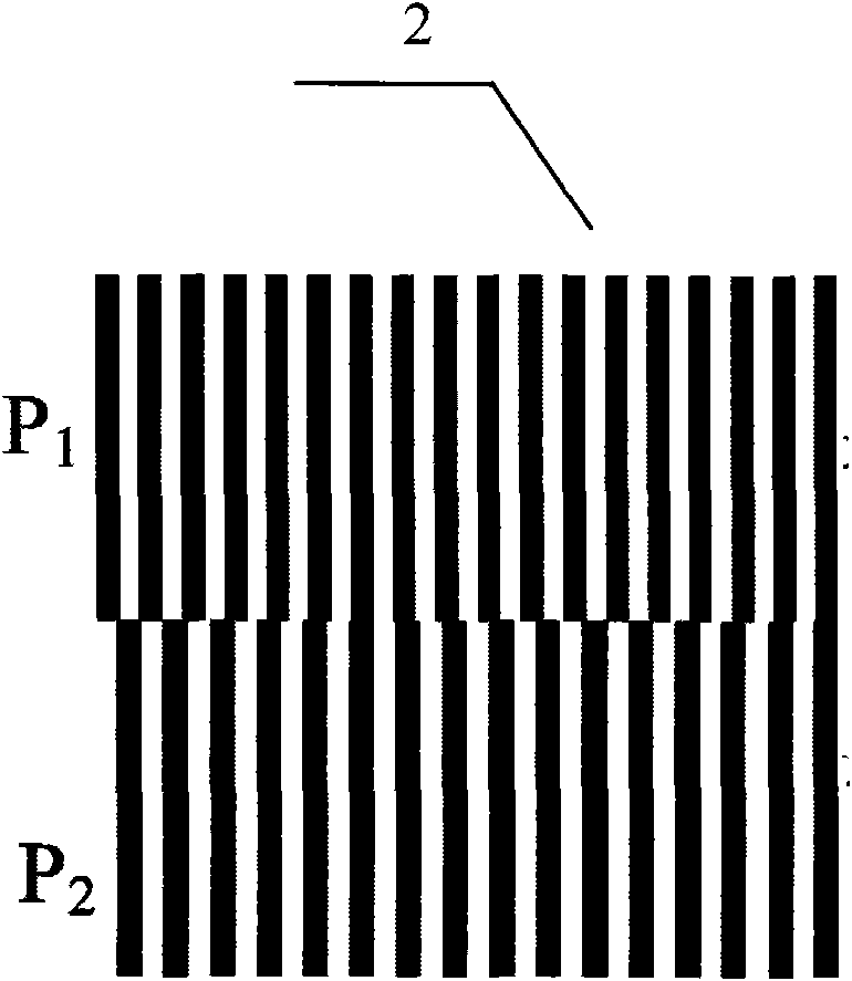
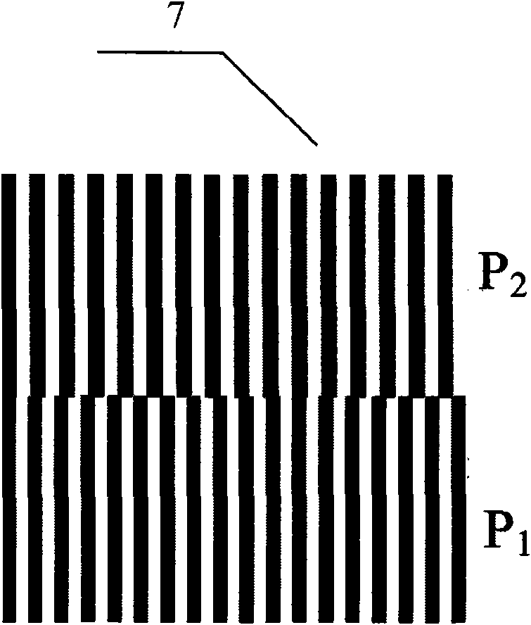
[0028] The present invention is used in projection lithography nanoscale automatic focusing system is composed of optical path A, image processing module 10 and circuit control module 11, wherein: as figure 1 As shown, the optical path A includes a collimated laser beam 1, a first grating mark 2, a first lens 3, a second lens 4, a third lens 5, a fourth lens 6, a second grating mark 7, a wafer stage 8 and a CCD Image detector 9; collimated laser beam 1 (in this embodiment, the wavelength of incident light is 633nm) vertically illuminates the first grating mark 2 located on the front focal plane of the first lens 3, and along the first lens 3 and the second lens 4 The optical axis of the formed first 4f system constitutes ...


PUM


Abstract

The invention relates to a nanometer-level automatic focusing system for projection lithography, comprising a light path, an image processing module and a circuit control module. The light path comprises a collimated light beam, two grating marks, four lenses, a silicon wafer stage and a CCD (Charge Coupled Device) image detector, wherein a collimated light beam vertically illuminates one grating mark, carries out glancing incidence imaging on the surface of the silicon wafer stage along the optic axes of the first lens and the second lens, is projected on the tested surface of the silicon wafer stage and undergoes mirror reflection; a grating image is reimaged on the focal plane of the fourth lens through the third lens and the fourth lens; and the image of one grating mark is superposed with the two grating marks by a fixed gap, undergoes multiple diffraction, forms amplified Moire interference fringes on the surface of the grating and then is imaged on the CCD image detector. The image processing module is used for processing images to extract a phase difference and further calculate a defocusing amount; and then, the circuit control module is used for judging the defocusing condition of the surface of the silicon wafer stage to further control the movement of the silicon wafer stage so that the surface of the silicon wafer stage reaches an optimal focal plane position.

Description

technical field [0001] The invention relates to a nanoscale automatic focusing system for projection lithography in lithography, in particular to an automatic focusing system for phase extraction using double gratings, and belongs to the related technical field of micro-nano processing. Background technique [0002] Optical lithography has always been the basis of large-scale integrated circuit industrial manufacturing technology. With the development of highly integrated circuits and related devices, the feature size of ICs is getting smaller and smaller, which continuously promotes the improvement of lithography resolution. However, with the improvement of resolution, the depth of focus problem in the exposure field is becoming more and more serious, and the accuracy of traditional focusing methods has been difficult to adapt to the gradually improved lithography resolution. [0003] The current focusing methods can generally be photometric focusing, CCD focusing and grati...

Claims


Application Information

Patent Timeline
IPC IPC(8): G03F7/20G03F9/00
Inventor 徐锋胡松罗正全周绍林陈旺富李金龙谢飞李兰兰盛壮
Owner INST OF OPTICS & ELECTRONICS - CHINESE ACAD OF SCI
Why Eureka
Try Eureka