Method for forming shallow trench isolation structure

A technology of isolation structures and shallow trenches, which is applied in the fields of electrical components, semiconductor/solid-state device manufacturing, circuits, etc., can solve the problems of low performance of semiconductor devices and affecting the electrical characteristics of semiconductor devices, etc. Good corrosion performance

Active Publication Date: 2011-08-10
SHANGHAI HUAHONG GRACE SEMICON MFG CORP
View PDF6 Cites 9 Cited by
  • Summary
  • Abstract
  • Description
  • Claims
  • Application Information

AI Technical Summary

Problems solved by technology

[0004] However, due to the defects of the existing shallow trench isolation structure, the area adjacent to the active region in the shallow trench will form a downward concave shape, called a side trench (Divot), which is formed on the substrate with the side trench formed. Semiconductor devices are prone to parasitic currents, which affect the electrical characteristics of semiconductor devices, and the existence of side trenches will lead to the formation of impurity residues (Residue) in the side trenches in the etching process of forming semiconductor devices, resulting in low performance of the formed semiconductor devices

Method used


Image

  • Method for forming shallow trench isolation structure
  • Method for forming shallow trench isolation structure
  • Method for forming shallow trench isolation structure

Examples


Embodiment Construction

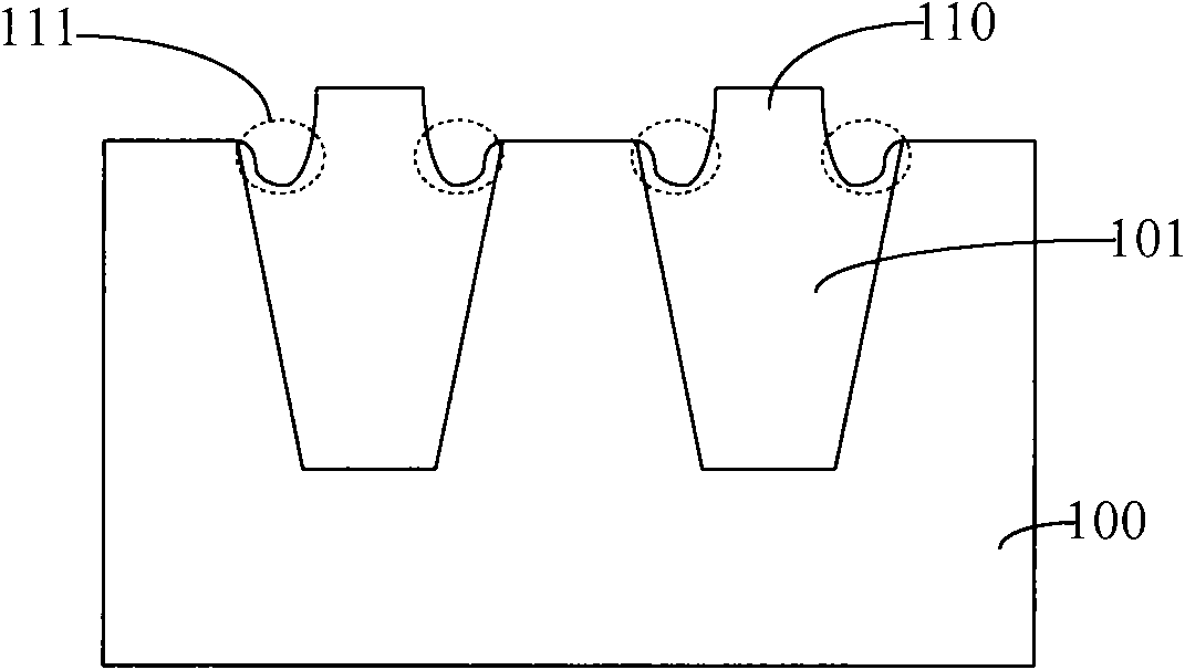
[0014] It can be seen from the background technology that in the existing shallow trench isolation structure, the isolation dielectric layer is located in a relatively loose area adjacent to the active region, which is corroded by the chemical reagents in the semiconductor device formation process, resulting in a gap between the shallow trench and the active region. The adjacent area will form a downward concave shape, called the side ditch (Divot), please refer to figure 1 , figure 1 The isolation shallow trench formed for the prior art includes a substrate 100; forming a shallow trench 101 in the substrate 100; a dielectric layer 110 filling the shallow trench; forming a side trench 111 in the dielectric layer, The semiconductor device formed by using the above-mentioned isolated shallow trenches is prone to generate parasitic current, thereby affecting the electrical characteristics of the semiconductor device, and the existence of side trenches will lead to the formation o...


PUM


Abstract

The invention discloses a method for forming a shallow trench isolation structure. The method comprises the following steps of: providing a substrate on which a gasket oxide layer and an etching stopping layer are formed sequentially, and forming a shallow trench in the substrate; forming an isolation medium layer which fills the shallow trench on the surfaces of the etching stopping layer and the gasket oxide layer; forming a first photoresist pattern on the surface of the isolation medium layer by using an active reverse mask; etching the isolation medium layer of partial thickness by using the first photoresist pattern as a mask; removing the isolation medium layer until the isolation medium layer is exposed out of the etching stopping layer by adopting a chemical mechanical polishing process after removing the first photoresist pattern; removing the etching stopping layer and the gasket oxide layer; forming a protection film which covers the isolation medium layer on the surface of the substrate; forming a second photoresist pattern on the surface of the protection film by using the active reverse mask; and removing the protection film until the protection film is exposed out of the substrate by using the second photoresist pattern as the mask to form a protection layer. A divot situation does not exist in the isolation of the shallow trench which is formed by the method.

Description

technical field [0001] The invention relates to the field of semiconductor manufacturing, in particular to a method for forming a shallow trench isolation structure. Background technique [0002] As semiconductor technology enters the deep submicron era, components below 0.18 microns, such as active regions of CMOS integrated circuits, are mostly made of shallow trench isolation structures for lateral isolation, which can also be found in US Patent No. US7112513 More information about Shallow Trench Isolation Technology. [0003] Shallow trench isolation structure as a device isolation technology, its specific process includes: forming a shallow trench on the substrate, the shallow trench is used to isolate the active region on the substrate, the formation method of the shallow trench It can be an etching process; fill the shallow trench with a medium, and form a medium layer on the surface of the substrate, the medium material can be silicon oxide; anneal the medium; use c...

Claims


Application Information

Patent Timeline
Patent Type & Authority Applications(China)
IPC IPC(8): H01L21/762
Inventor 张瑛林伟铭
Owner SHANGHAI HUAHONG GRACE SEMICON MFG CORP
Why Eureka
Try Eureka