Alloy wire for connecting semiconductor components

A semiconductor and alloy wire technology, which is applied in the direction of semiconductor devices, semiconductor/solid-state device parts, electric solid-state devices, etc., can solve problems such as uneven loops, easy bending of lead frames, and bonding problems between alloy wires and lead frames.

Inactive Publication Date: 2011-08-17
DONGGUAN ZHENGQI ELECTRONICS
View PDF5 Cites 13 Cited by
  • Summary
  • Abstract
  • Description
  • Claims
  • Application Information

AI Technical Summary

Problems solved by technology

Although the high temperature of heating at this time helps to improve the adhesion, it also makes the lead frame easy to bend, and it is easy to produce uneven shapes of the circuit
[0004] However, if the heating temperature is too low, altho

Method used


Image

  • Alloy wire for connecting semiconductor components
  • Alloy wire for connecting semiconductor components

Examples


Embodiment Construction

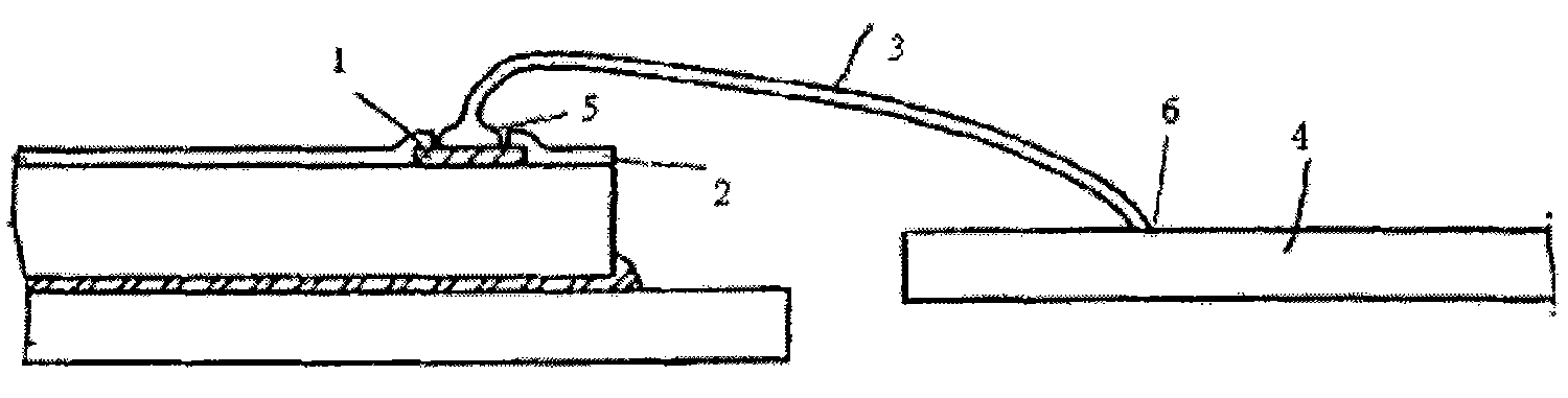
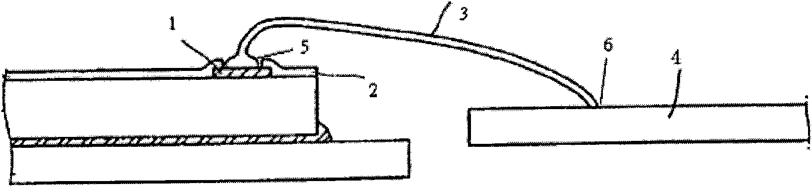
[0019] In the following examples, the preparation method is as follows: Add a certain amount of other elements to high-purity silver with a purity of 99.999% (weight percent), and after vacuum melting, cast an alloy rod with the indicated composition, and roll, wire draw Machine cold forming and intermediate annealing, and finally cold forming into a thin wire with a diameter of 18 μm and final annealing to achieve an elongation of 10-15%. Using the automatic wire bonding machine model 1488 of K&S Company, the alloy wire is bonded between IC, LED chip Al, Au electrode and copper alloy lead frame at a heating temperature of 100 ° C by using ultrasonic combined hot pressing method. For bonding work, make a bonding sample of 100 pins. Then, after sealing the sample with epoxy resin, a thermal cycle test of -20°C x 30 minutes and 180°C x 30 minutes was carried out one hundred times.

[0020] (1) 0.4-15% by weight of gold (Au), at least one of 0.2-5% by weight of palladium (Pd) or...


PUM


Abstract

The invention discloses an alloy wire for connecting semiconductor components, which is characterized in that the alloy contains the following contents according to the weight percentage: 0.4 to 15% of gold, 0.2 to 5% of at least one of palladium and platinum, 0.0001 to 0.05% of at least one of Y, La, Ru, Ir, Eu, Yb, Gb and Be, and the rest of silver and inevitable impurities. The alloy wire can increase connectivity, peel strength and vibration fracture of a second side edge.

Description

technical field [0001] The invention relates to an alloy wire for connecting semiconductor components. Background technique [0002] In the prior art, the technology of connecting electrodes and external wires of semiconductor components such as transistors, ICs, LSIs, and LEDs uses gold wires made of high-purity gold with a proportion of more than 99.99% and other trace metal elements as connecting wires. It is mainly to adopt ultrasonic wave and use hot pressing connection method. Wiring with ultrasonic wave and hot pressing connection method, the formed circuit is as follows figure 1 shown. 1 is IC and LED chip, 2 is Al and Au electrodes on IC and LED chip, 3 is alloy wire, 4 is lead frame, 5 is the first side joint, 6 is the second side joint. [0003] Recently, the installation of semiconductors is based on the heat dissipation and cost of the external lead material, so the lead frame made of copper alloy is mostly used. When using a lead frame made of copper alloy,...

Claims


Application Information

Patent Timeline
IPC IPC(8): C22C5/06C22C5/08H01L23/49
CPCH01L2924/01063H01L2924/01044H01L2924/0107H01L2924/01057H01L2924/01082H01L2924/01064H01L2224/45144H01L2924/01013H01L2224/45139H01L2224/02166H01L2924/01029H01L2924/01047H01L2224/48247H01L2924/01004H01L2924/01046H01L2224/48465H01L2924/01019H01L24/45H01L2924/01006H01L2924/01078H01L2924/01077H01L2924/01079H01L2224/43848H01L2224/45015H01L24/43H01L2224/73265H01L2924/00011H01L2224/45H01L2224/43H01L2924/01039H01L2924/00H01L2924/00015H01L2924/01204H01L2924/013H01L2924/20751H01L2924/20752H01L2924/20753H01L2924/20754H01L2924/20755H01L2924/20756H01L2924/20757H01L2924/20758H01L2924/20759H01L2924/01049H01L2924/2076H01L2924/00012H01L2224/32245
Inventor 何守仁
Owner DONGGUAN ZHENGQI ELECTRONICS
Why Eureka
Try Eureka